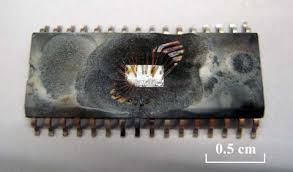
Unlock Microcontroller PIC16LF946 Protected Heximal
PORTA is a 8-bit wide, bidirectional port which is useful in the process of Unlock Microcontroller PIC16LF946 Protected Heximal. The corresponding data direction register is TRISA (Register 3-2). Setting a TRISA bit (= 1) will make the corresponding PORTA pin an input (i.e., put the corresponding output driver in a High-impedance mode).
Clearing a TRISA bit (= 0) will make the corresponding PORTA pin an output (i.e., put the contents of the output latch on the selected pin). Example 3-1 shows how to initialize PORTA.
Five of the pins of PORTA can be configured as analog inputs to facilitate MCU Reading. These pins, RA5 and RA<3:0>, are configured as analog inputs on device power-up and must be reconfigured by the user to be used as I/O’s. This is done by writing the appropriate values to the CMCON0 and ANSEL registers (see Example 3-1) before .

Unlock Microcontroller PIC16LF946 Protected Heximal
Reading the PORTA register (Register 3-1) reads the status of the pins similar with Read IC PIC MCU PIC16F887, whereas writing to it will write to the port latch. All write operations are read-modify-write operations. Therefore, a write to a port implies that the port pins are read, this value is modified and then written to the port data latch.
The TRISA register controls the direction of the PORTA pins, even when they are being used as analog inputs. The user must ensure the bits in the TRISA register are maintained set when using them as analog inputs.
I/O pins configured as analog input always read “0” Each PORTA pin is multiplexed with other functions in order to Break Locked MCU PIC16C74B Eeprom Memory. The pins and their combined functions are briefly described here. For specific information about individual functions, refer to the appropriate section in this data sheet of MCU PIC16LF946.
Below Figure shows the diagram for this pin. The RA2/AN2/C2+/VREF-/COM2 pin is configurable to function as one of the following:
a general purpose I/O
an analog input for the A/D
an analog input for Comparator 2
a voltage reference input for the A/D
an analog output for the LCD
Figure 3-4 shows the diagram for this pin. The RA3/AN3/C1+/VREF+/COM3/SEG15 pin is configurable to function as one of the following:
a general purpose input
an analog input for the A/D
an analog input from Comparator 1
a voltage reference input for the A/D
analog outputs for the LCD

