Unlock Microcontroller AT89C51RC2 Eeprom
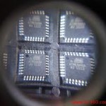
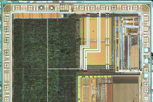
Unlock Microcontroller AT89C51RC2 to recover eeprom memory data from MCU, copy heximal to new MCU AT89C51RC2 to a perfect MCU cloning;
With EXTRAM = 0, the XRAM is indirectly addressed, using the MOVX instruction in combination with any of the registers R0, R1 of the selected bank or DPTR. An access to XRAM will not affect ports P0, P2, P3.6 (WR) and P3.7 (RD) when reading Microcontroller pic16c717 program.
For example, with EXTRAM = 0, MOVX @R0, # data where R0 contains 0A0H, accesses the XRAM at address 0A0H rather than external memory.
An access to external data memory locations higher than the accessible size of the XRAM will be performed with the MOVX DPTR instructions in the same way as in the standard 80C51, with P0 and P2 as data/address busses, and P3.6 and P3.7 as write and read timing signals. Accesses to XRAM above 0FFH can only be done by the use of DPTR.
With EXTRAM = 1, MOVX @RI and MOVX @DPTR will be similar to the standard 80C51. MOVX @ Ri will provide an eight-bit address multiplexed with data on Port0 and any output port pins can be used to output higher order address bits after crack ic pic16c771 firmware.
This is to provide the external paging capability. MOVX @DPTR will generate a sixteen-bit address. Port2 outputs the high-order eight address bits (the contents of DPH) while Port0 multiplexes the low-order eight address bits (DPL) with data. MOVX @ RI and MOVX @DPTR will generate either read or write signals on P3.6 (WR) and P3.7 (RD).
The stack pointer (SP) may be located anywhere in the 256 Bytes RAM (lower and upper RAM) internal data memory. The stack may not be located in the XRAM. The M0 bit allows to stretch the XRAM timings; if M0 is set, the read and write pulses are extended from 6 to 30 clock periods. This is useful to access external slow peripherals when crack Microcontroller pic16c716 heximal.
The Timer 2 in the AT89C51RB2/RC2 is the standard C52 Timer 2. It is a 16-bit timer/counter: the count is maintained by two eight-bit timer registers, TH2 and TL2 are cascaded. It is controlled by T2CON (Table 20) and T2MOD (Table 21) registers.
Timer 2 operation is similar to Timer 0 and Timer 1C/T2 selects FOSC/12 (timer operation) or external pin T2 (counter operation) as the timer clock input. Setting TR2 allows TL2 to increment by the selected input.
Timer 2 has 3 operating modes: capture, autoreload and Baud Rat e Generator. These modes are selected by the combination of RCLK, TCLK and CP/RL2 (T2CON). see the Atmel 8-bit Microcontroller Hardware description for the description of Capture and Baud Rate Generator Modes.
Timer 2 includes the following enhancements:
Auto-reload mode with up or down counter
Programmable clock-output
The auto-reload mode configures Timer 2 as a 16-bit timer or event counter with automatic reload. If DCEN bit in T2MOD is cleared, Timer 2 behaves as in 80C52 (see the Atmel C51 Microcontroller Hardware description). If DCEN bit is set, Timer 2 acts as an Up/down timer/counter as shown in Figure 8. In this mode the T2EX pin controls the direction of count.
When T2EX is high, Timer 2 counts up. Timer overflow occurs at FFFFh which sets the TF2 flag and generates an interrupt request. The overflow also causes the 16-bit value in RCAP2H and RCAP2L registers to be loaded into the timer registers TH2 and TL2.
When T2EX is low, Timer 2 counts down. Timer underflow occurs when the count in the timer registers TH2 and TL2 equals the value stored in RCAP2H and RCAP2L registers. The underflow sets TF2 flag and reloads FFFFh into the timer registers.
The EXF2 bit toggles when Timer 2 overflows or underflows according to the direction of the count. EXF2 does not generate any interrupt. This bit can be used to provide 17-bit resolution when Unlock Microcontroller.
Tags: unlock microcontroller binary archive,unlock microcontroller binary code,unlock microcontroller binary content,unlock microcontroller binary data,unlock microcontroller binary eeprom,unlock microcontroller binary file,unlock microcontroller binary firmware,unlock microcontroller binary information,unlock microcontroller binary memory,unlock microcontroller binary program


