Unlock Microcontroller AT89C51CC01 Flash
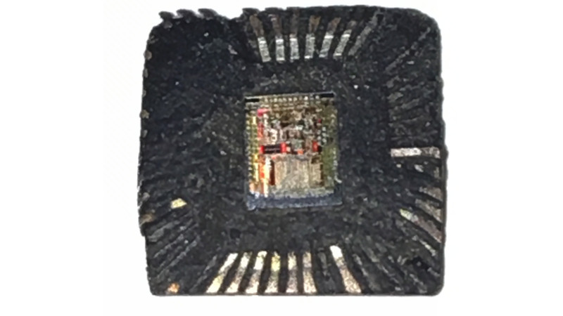
Unlock Microcontroller AT89C51CC01 Flash memory and read flash content from mcu at89c51cc01 memory, the fuse bit of MCU will be break to disable the protection;
The T89C51CC01 core needs only 6 clock periods per machine cycle. This feature, called ”X2”, provides the following advantages:
Divides frequency crystals by 2 (cheaper crystals) while keeping the same CPU power. Saves power consumption while keeping the same CPU power (oscillator power saving). Saves power consumption by dividing dynamic operating frequency by 2 in operating and idle modes. Increases CPU power by 2 while keeping the same crystal frequency when discover avr Microcontroller atmega162 .
In order to keep the original C51 compatibility, a divider-by-2 is inserted between the XTAL1 signal and the main clock input of the core (phase generator). This divider may be disabled by the software.
An extra feature is available to start after Reset in the X2 mode. This feature can be enabled by a bit X2B in the Hardware Security Byte. This bit is described in the section “In-System-Programming”.
The X2 bit in the CKCON register (see Table 13) allows switching from 12 clock cycles per instruction to 6 clock cycles and vice versa. At reset, the standard speed is activated (STD mode).
Setting this bit activates the X2 feature (X2 mode) for the CPU Clock only (see Figure 5.) before reverse pld altera epm7064LC44.
The Timers 0, 1 and 2, Uart, PCA, Watchdog or CAN switch in X2 mode only if the corresponding bit is cleared in the CKCON register. The clock for the whole circuit and peripheral is first divided by two before being used by the CPU core and peripherals. This allows any cyclic ratio to be accepted on the XTAL1 input. In X2 mode, as this divider is bypassed, the signals on XTAL1 must have a cyclic ratio between 40 to 60%. Figure 5. shows the clock generation block diagram after reverse R5F21388CNFP Microcontroller .
The X2 bit is validated on the XTAL1÷2 rising edge to avoid glitches when switching from the X2 to the STD mode. Figure 6 shows the mode switching waveforms.
Two power reduction modes are implemented in the T89C51CC01: the Idle mode and the Power-down mode. These modes are detailed in the following sections. In addition to these power reduction modes, the clocks of the core and peripherals can be dynamically divided by 2 using the X2 Mode detailed in Section “Clock”.
In order to start-up (cold reset) or to restart (warm reset) properly the microcontroller, a high level has to be applied on the RST pin. A bad level leads to a wrong initialisation of the internal registers like SFRs, PC, etc. and to unpredictable behavior of the microcontroller. A warm reset can be applied either directly on the RST pin or indirectly by an internal reset source such as a watchdog, PCA, timer, etc.
Two conditions are required before enabling a CPU start-up: VDD must reach the specified VDD range, The level on xtal1 input must be outside the specification (VIH, VIL). If one of these two conditions are not met, the microcontroller does not start correctly and can execute an instruction fetch from anywhere in the program space. An active level applied on the RST pin must be maintained until both of the above conditions are met. A reset is active when the level VIH1 is reached and when the pulse width covers the period of time where VDD and the oscillator are not stabilized. Two parameters have to be taken into account to determine the reset pulse width when Unlock Microcontroller :
VDD rise time (vddrst),
Oscillator startup time (oscrst). To determine the capacitor the highest value of these two parameters has to be chosen. The reset circuitry is shown in Figure 7.
Tags: unlock microcontroller embedded archive,unlock microcontroller embedded code,unlock microcontroller embedded content,unlock microcontroller embedded data,unlock microcontroller embedded eeprom,unlock microcontroller embedded file,unlock microcontroller embedded firmware,unlock microcontroller embedded information,unlock microcontroller embedded memory,unlock microcontroller embedded program


