Unlock MCU ST10F272Z2T3 Chip Flash Memory Firmware
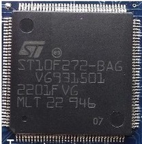
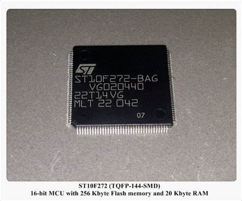
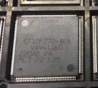
Unlock MCU ST10F272Z2T3 Chip Flash Memory Firmware from its memory and then copy binary software to new microcontroller ST10F272Z2; the new microprocessor ST10F272 can provide the exactly same functions as original ones;

The architecture of the ST10F273 combines advantages of both RISC and CISC processors and an advanced peripheral subsystem. The block diagram gives an overview of the different on-chip components and the high bandwidth internal bus structure of the ST10F272.

The memory space of the ST10F273 is configured in a unified memory architecture. Code memory, data memory, registers and I/O ports are organized within the same linear address space of 16 Mbytes to clone mcu st10f272 flash memory program. The entire memory space can be accessed Byte wise or Word wise. Particular portions of the on-chip memory have additionally been made directly bit addressable.

IFlash: 512 Kbytes of on-chip Flash memory. It is divided in 10 blocks (B0F0…B0F9) of the Bank 0 and two blocks of Bank 1 (B1F0, B1F1): read-while-write operations inside the same Bank are not allowed. When Bootstrap mode is selected to crack secured microcontroller st10f272 flash memory, the Test-Flash Block B0TF (8 Kbyte) appears at address 00’0000h: refer to Chapter 5: Internal Flash memory on page 25 for more details on memory mapping in boot mode. The summary of address range for IFlash is the following:

