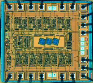
Samsung S3F9498 Microcontroller Heximal Cloning
The upper 72 bytes of the S3F9498’s internal register file are addressed as working registers, system control registers and peripheral control registers, all of these 3 registers are useful for Samsung S3F9498 Microcontroller Heximal Cloning. The lower 184 bytes of internal register file (00H–B7H) is called the general purpose register space.
For many SAMSUNG microcontrollers, the addressable area of the internal register file is further expanded by the additional of one or more register pages at general purpose register space (00H–BFH). This register file expansion is implemented by page 1 in the S3F9498 to faciliate the process of IC breaking. The page 1 (20 8 bits) is for LCD display register and can be used as general-purpose registers.
The SAMSUNG register architecture provides an efficient method of working register addressing that takes full advantage of shorter instruction formats to reduce execution time when Break MC68HC908EY16 Microprocessor Protected Flash.
This16-byte address range is called common area. That is, locations in this area can be used as working registers by operations that address any location on any page in the register file. Typically, these working registers serve as temporary buffers for data operations between different pages in order to Crack MCU IC NXP LPC2361.
The Register (R) addressing mode can be used to access this area
Registers are addressed either as a single 8-bit register or as a paired 16-bit register. In 16-bit register pairs, the address of the first 8-bit register is always an even number and the address of the next register is an odd number. The most significant byte of the 16-bit data is always stored in the even-numbered register; the least significant byte is always stored in the next (+ 1) odd-numbered register similar to the process of Extract AVR Microcontroller ATmega8515.


