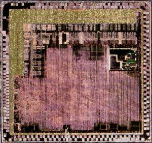
Restore MCU Microchip SST89E58RD2A
Restore MCU Microchip SST89E58RD2ARestore MCU Microchip SST89E58RD2A, below please find the features for your reference:
| SST89E/V58 / 54 / 52RD2/RD FlashFlex51 MCU
Preliminary FEATURES: |
| · 8-bit 8051-Compatible Microcontroller (MCU) · Ten Interrupt Sources at 4 Priority
with Embedded SuperFlash Memory – Four External Interrupt Inputs – Fully Software Compatible · Programmable Watchdog Timer – Development Toolset Compatible · Programmable Counter Array (PCA) – Pin-For-Pin Package Compatible · Four 8-bit I/O Ports (32 I/O Pins) · SST89E5xRD2 Operation One 4-bit Port – 0 to 40 MHz at 5V · Second DPTR register · SST89V5xRD2 Operation · Low EMI Mode (Inhibit ALE) – 0 to 33 MHz at 3V · SPI Serial Interface · 1 KByte Internal RAM · Standard 12 Clocks per cycle, the · Dual Block SuperFlash EEPROM option to double the speed to 6 – 8/16/32 KByte primary block + · TTL- and CMOS-Compatible Logic 8 KByte secondary block · Brown-out Detection (128-Byte sector size for both blocks) · Low Power Modes – Individual Block Security Lock with SoftLock – Concurrent Operation during – Power-down Mode with External In-Application Programming (IAP) – Idle Mode – Memory Overlay for Interrupt Support during IAP · Temperature Ranges: · Support External Address Range up to 64 – Commercial (0°C to +70°C) KByte of Program and Data Memory – Industrial (-40°C to +85°C) · Three High-Current Drive Ports (16 mA each) · Packages Available · Three 16-bit Timers/Counters – 44-lead PLCC · Full-Duplex, Enhanced UART – 40-pin PDIP (Port 4 feature not – 44-lead TQFP – Framing Error Detection – Automatic Address Recognition · All non-Pb (lead-free) devices are |
| PRODUCT DESCRIPTION
The SST89E5xRD2/RD and SST89V5xRD2/RD are In addition to the 16/24/40 KByte of members of the FlashFlex51 family of 8-bit microcontroller memory on-chip, the devices can address products designed and manufactured with SST’s patented of external program memory. In addition to and proprietary SuperFlash CMOS semiconductor pro- on-chip RAM, up to 64 KByte of external access technology. The split-gate cell design and thick-oxide addressed. tunneling injector offer significant cost and reliability bene- The flash memory blocks can be fits for SST’s customers. The devices use the 8051 instruc dard 87C5x OTP EPROM programmer fitted tion set and are pin-for-pin compatible with standard 8051 adapter and the firmware for SST’s devices. microcontroller devices. on reset, the devices can be configured as The devices come with 16/24/40 KByte of on-chip flash an external host for source code storage or EEPROM program memory which is partitioned into 2 external host for an in-application independent program memory blocks. The primary Block 0ation. The devices are designed to be occupies 8/16/32 KByte of internal program memory space tem and in-application on the printed and the secondary Block 1 occupies 8 KByte of internal maximum flexibility. The devices are program memory space. an example of the bootstrap loader in the strating the initial user program code loading The 8-KByte secondary block can be mapped to the lowest user code updating via the IAP operation. location of the 8/16/32 KByte address space; it can also be bootstrap loader is available for the user’s hidden from the program counter and used as an indepen-convenience only; SST does not guarantee dent EEPROM-like data memory. or usefulness. Chip-Erase or Block-Erase erase the pre-programmed sample code. |
Tags: restore mcu code,restore mcu firmware,restore mcu flash,restore mcu memory,restore mcu program,копирам mcu binary,копирам mcu code,копирам mcu data,копирам mcu eeprom,копирам mcu file,копирам mcu firmwre,копирам mcu flash,копирам mcu heximal,копирам mcu memory,копирам mcu program


