-
Product Categories
Live Support Chat


Restore MCU DSC IC Texas Instrument TMS320F28232PGFA
The Texas Instruments TMS320F28232PGFA is a secured Digital Signal Controller (DSC) used in industrial and embedded applications. This microcontroller (MCU) integrates protected memory blocks, including flash, EEPROM, and binary files, to prevent unauthorized access. However, researchers, engineers, and security analysts may need to restore the MCU for legitimate purposes such as data recovery, program duplication, or reverse engineering. This article explores various techniques to crack and extract data from the TMS320F28232PGFA;
Methods to Break the Protection of TMS320F28232PGFA
Reverse Engineering Attack
Reverse engineering the TMS320F28232PGFA involves analyzing its chip architecture, memory layout, and security mechanisms. This method requires a deep understanding of the MCU’s EEPROM and flash memory, allowing the researcher to locate potential vulnerabilities that can be exploited to decrypt and decode the locked firmware.
Voltage Glitching & Fault Injection
This technique applies sudden voltage fluctuations to disrupt the protected execution process of the MCU. The idea is to induce errors at the right moment, allowing unauthorized access to extract the secured data. Voltage glitching can sometimes disable the security mechanisms temporarily, making it possible to dump the flash or EEPROM contents.
JTAG Debugging & Interface Exploitation
Some Texas Instruments MCUs, including the TMS320F28232PGFA, feature JTAG or UART debugging ports. If the debugging interface is not fully locked, it may be possible to open access and extract the binary program. Specialized tools can crack the protection, enabling data dumping and cloning the firmware onto another MCU.
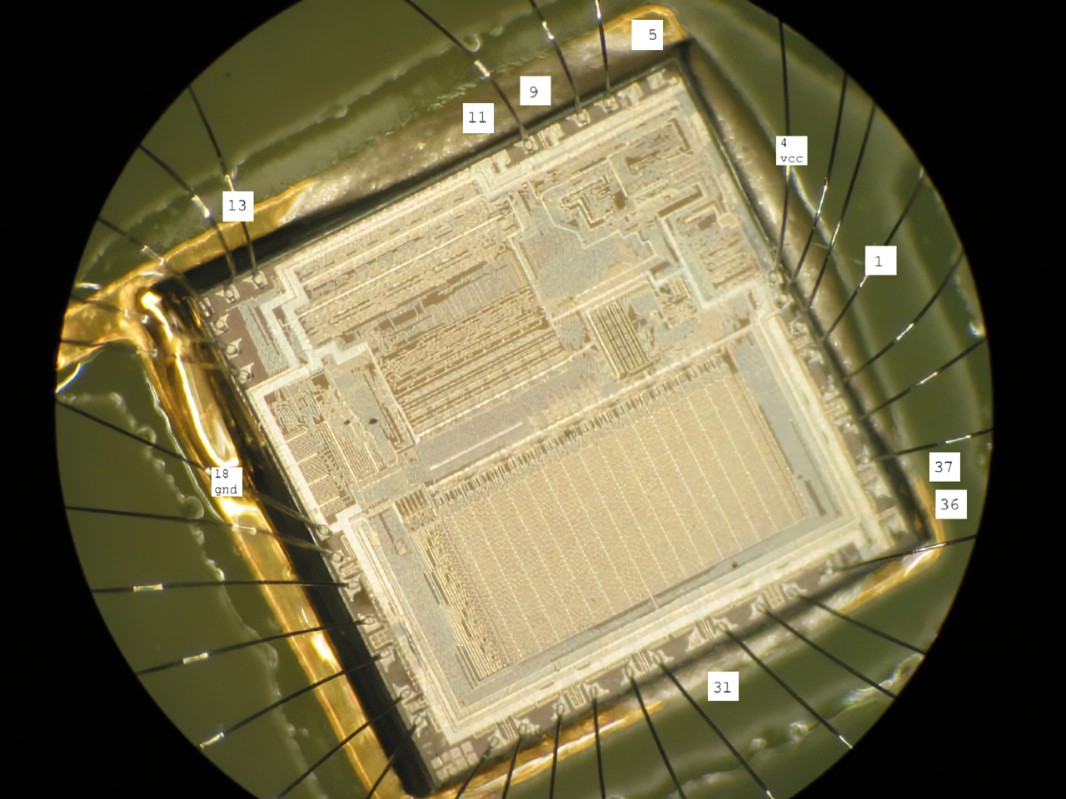
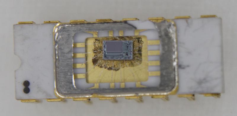
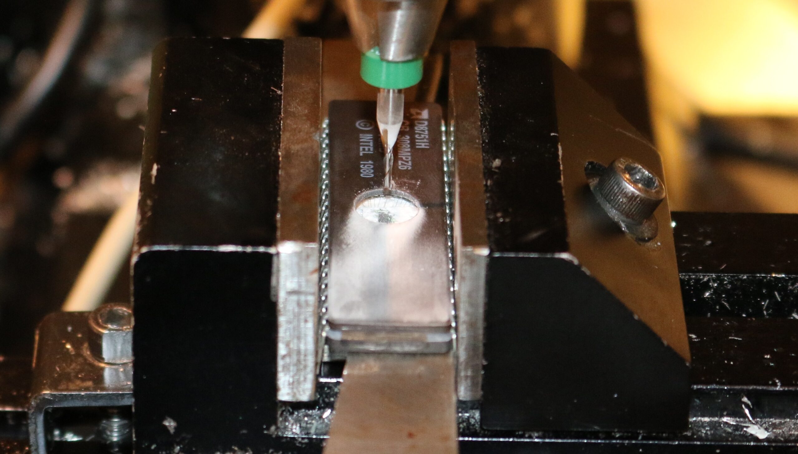
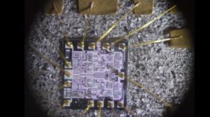
Chip Decapsulation & Microprobing
Decapsulation is a highly advanced physical attack technique where the protective layer of the microprocessor is chemically removed to expose internal circuits. Using microprobing, researchers can directly tap into the memory bus and capture raw heximal data. This method is expensive and requires specialized laboratory equipment.
EEPROM Dumping & Code Extraction
If partial firmware backup is possible, engineers can attempt to reconstruct the source code using disassemblers and decompilers. This approach allows for replication and duplication of the program logic even if the full binary file cannot be retrieved.
Legal and Ethical Considerations
While these techniques may be used to restore lost firmware, any attempt to break, decrypt, or hack a protected MCU without authorization is illegal. Always ensure compliance with legal regulations before performing any attack or extraction.
We can Restore MCU DSC IC Texas Instrument TMS320F28232PGFA, please view chip features below for your reference:
· High-Performance Static CMOS Technology
– Up to 150 MHz (6.67-ns Cycle Time)
– 1.9-V/1.8-V Core, 3.3-V I/O Design
· High-Performance 32-Bit CPU (TMS320C28x)
– IEEE-754 Single-Precision Floating-Point
– 16 x 16 and 32 x 32 MAC Operations
– 16 x 16 Dual MAC
– Harvard Bus Architecture
– Fast Interrupt Response and Processing
– Unified Memory Programming Model
– Code-Efficient (in C/C++ and Assembly)
· Six-Channel DMA Controller (for ADC, McBSP, ePWM, XINTF, and SARAM)
· 16-Bit or 32-Bit External Interface (XINTF)
– Over 2M x 16 Address Reach
· On-Chip Memory
– F28335, F28235:
256K x 16 Flash, 34K x 16 SARAM
– F28334, F28234:
128K x 16 Flash, 34K x 16 SARAM
– F28332, F28232:
64K x 16 Flash, 26K x 16 SARAM
– 1K x 16 OTP ROM
· Boot ROM (8K x 16)
– With Software Boot Modes (via SCI, SPI, CAN, I2C, McBSP, XINTF, and Parallel I/O)
· Clock and System Control
– Dynamic PLL Ratio Changes Supported
– On-Chip Oscillator
– Watchdog Timer Module
· GPIO0 to GPIO63 Pins Can Be Connected to One of the Eight External Core Interrupts
· Peripheral Interrupt Expansion (PIE) Block That Supports All 58 Peripheral Interrupts
· 128-Bit Security Key/Lock
– Protects Flash/OTP/RAM Blocks
– Prevents Firmware Reverse Engineering
· Enhanced Control Peripherals
– Up to 6 HRPWM Outputs With 150 ps MEP Resolution
– Up to 6 Event Capture Inputs
– Up to 2 Quadrature Encoder Interfaces
– Up to 8 32-Bit Timers
– Up to 9 16-Bit Timers
(6 for ePWMs and 3 XINTCTRs)
· Three 32-Bit CPU Timers
· Serial Port Peripherals
– Up to 2 CAN Modules
– Up to 3 SCI (UART) Modules
– Up to 2 McBSP Modules (Configurable as SPI)
– One Inter-Integrated-Circuit (I2C) Bus
· 12-Bit ADC, 16 Channels
– 80-ns Conversion Rate
– 2 x 8 Channel Input Multiplexer
– Two Sample-and-Hold
– Single/Simultaneous Conversions
– Internal or External Reference
· Up to 88 Individually Programmable, Multiplexed GPIO Pins With Input Filtering
· JTAG Boundary Scan Support (1)
· Advanced Emulation Features
– Analysis and Breakpoint Functions
– Real-Time Debug via Hardware
· Development Support Includes
– ANSI C/C++ Compiler/Assembler/Linker
– Code Composer Studio™ IDE
– DSP/BIOS™
– Digital Motor Control and Digital Power Software Libraries
Low-Power Modes and Power Savings
– IDLE, STANDBY, HALT Modes Supported
– Disable Individual Peripheral Clocks
· Endianness: Little Endian
· Package Options:
– Lead-free, Green Packaging
– Low-Profile Quad Flatpack (PGF, PTP)
– MicroStar BGA™ (ZHH)
· Temperature Options:
– A: –40°C to 85°C (PGF, ZHH, ZJZ)
– S: –40°C to 125°C (PTP, ZJZ)
– Q: –40°C to 125°C (PTP, ZJZ)