Replicate ST MicroProcessor ST7FMC2N6B3 Firmware
We can Replicate ST MicroProcessor ST7FMC2N6B3 Firmware, please view the MicroProcessor ST7FMC2N6B3 features for your reference:
- MCCFI can be mapped on 2 different pins on 80 ,64 and 56-pin packages. This allows:
- – either to use PC1 as a standard I/O and map MCCFI on OAZ (MCCFI1) with or without using the oper- ational amplifier (selected case after reset),
- – or to map MCCFI on PC1 (MCCFI0) and use the amplifier for another Replicate ST MicroProcessor ST7FMC2N6B3 Firmware
The mapping can be selected in MREF register of motor control cell. See section MOTOR CONTROL for more details.
- MCZEM is mapped on PF1 on 80, 64 and 56-pin packages and on PD2 on 44 and 32-pins. MCDEM is mapped on PF0 on 80, 64 and 56-pin packages and on PD1 on 44 and 32-pin packages.
- MCPWMV is mapped on PC6 on 80 and 64-pin packages and on PD1 on 44,and 32-pins packages. MCPWMW is mapped on PC7 on 80, 64 and 44-pin packages and on PD0 on 32-pins package.
- Once the MTC peripheral is ON (bits CKE=1 or DAC=1 in the register MCRA), the pin PC4 is configured to an alternate function. PC4 is no longer usable as a digital I/O before Replicate ST MicroProcessor ST7FMC2N6B3 Firmware.
On the chip, each I/O port has 8 pads. Pads that are not bonded to external pins are in input pull-up configuration after reset. The configuration of these pads must be kept at reset state to avoid added cur- rent consumption.
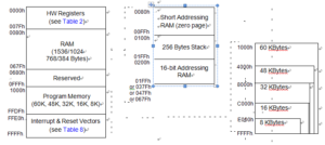
As shown in below Figure, the MCU is capable of ad- dressing 64K bytes of memories and I/O registers.
The available memory locations consist of 128 bytes of register locations, up to 2Kbytes of RAM and up to 60Kbytes of user program memory. The RAM space includes up to 256 bytes for the stack from 0100h to 01FFh after CRACK MCU.


