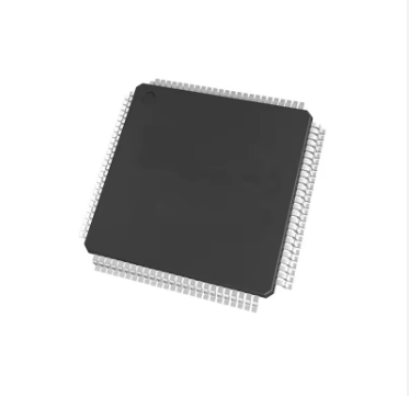
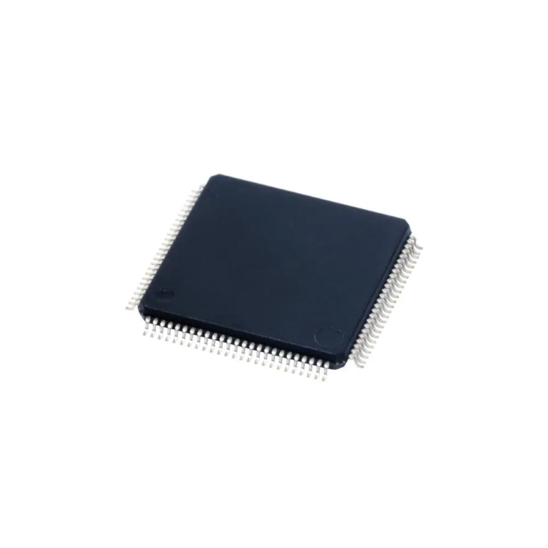
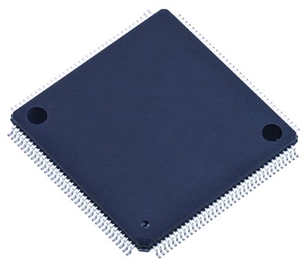
Renesas Microprocessor R5F64168DFB Flash Code Duplication
Renesas Microprocessor R5F64168DFB Flash Code Duplication will help engineer to recover MCU firmware out from its flash memory after disable the securitive fuse bits over the microcontroller and by injecting faulting onto the Center processing unit to interrupe the execution of Microcontroller;

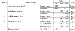
Please check below Electrical Characteristics of Flash Memory:

Program/erase definition
This value represents the number of erasures per block.
When the number of program/erase cycles is n, each block can be erased n times.

For example, if a 4-word write is performed in 512 different addresses in the 4-Kbyte block A and then the block is erased, this is counted as a single program/erase operation especially for Microcontroller ATtiny4313A Heximal unlocking.
However, the same address cannot be written to more than once per erasure (overwrite disabled).

Data retention includes periods when no supply voltage is applied and no clock is provided;
The MCU uses the standard 740 family instruction set. Refer to the table of 740 family addressing modes and machine-language instructions or the SERIES 740 <SOFTWARE> USER’S MANUAL for details on each instruction set.
Machine-resident 740 family instructions are as follows:
1. The FST and SLW instructions cannot be used.
2. The MUL and DIV instructions can be used.
3. The WIT instruction can be used.
4. The STP instruction can be used.
The accumulator is an 8-bit register. Data operations such as data transfer, etc., are executed mainly through the accumulator.
Both index register X and index register Y are 8-bit registers. In the index addressing modes, the value of the OPERAND is added to the contents of register X or register Y and specifies the real address when Crack Renesas MCU M37542F8GP Flash.

When the T flag in the processor status register is set to “1”, the value contained in index register X becomes the address for the second OPERAND.

