Renesas MCU R5F21324CNSP Flash Program Copying
Renesas MCU R5F21324CNSP Flash Program Copying is a process starts from break off the protection over r5f21324cn locked mcu flash memory,

A0 is a 16-bit register for address register indirect addressing and address register relative addressing. It is also used for transfer and arithmetic and logic operations. A1 is analogous to A0. A1 can be combined with A0 and used as a 32-bit address register (A1A0).
The I flag enables maskable interrupts. Interrupts are disabled when the I flag is set to 0, and are enabled when the I flag is set to 1 in order to clone microcontroller NEC R5F21276JFP heximal file. The I flag is set to 0 when an interrupt request is acknowledged.
ISP is selected when the U flag is set to 0; USP is selected when the U flag is set to 1. The U flag is set to 0 when a hardware interrupt request is acknowledged or the INT instruction of software interrupt numbers 0 to 31 is executed.

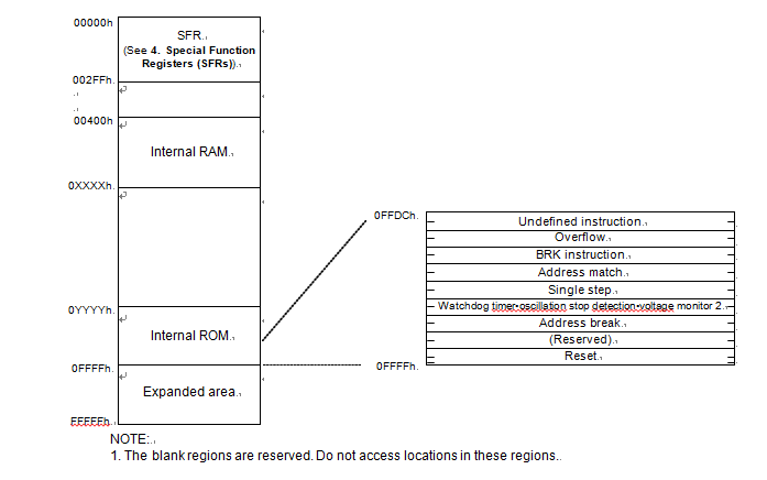
Below Figure is a Memory Map of R8C/1A Group. The R8C/1A Group has 1 Mbyte of address space from addresses 00000h to FFFFFh.
The internal ROM is allocated lower addresses, beginning with address 0FFFFh. For example, a 16- Kbyte internal ROM area is allocated addresses 0C000h to 0FFFFh when cloning renesas mcu r5f21192sp flash memory content. The fixed interrupt vector table is allocated addresses 0FFDCh to 0FFFFh. They store the starting address of each interrupt routine.


