-
Product Categories
Live Support Chat


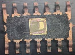
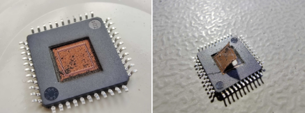
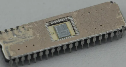
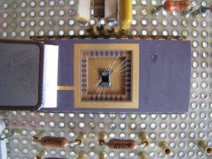
Recover Locked STM32F102RB MCU Program
When dealing with a locked STM32F102RB MCU, recovering the program can be a complex yet essential task. The microcontroller’s firmware is often protected or encrypted to prevent unauthorized access or modification. However, there are several techniques that can be employed to crack or unlock the MCU, enabling you to extract the binary data, firmware, or source code.
One common method is reverse engineering the chip, which involves analyzing the microprocessor to find vulnerabilities that may allow you to bypass security measures. By using specialized attack techniques, such as voltage glitching or timing analysis, it’s possible to decrypt or decode the secured flash memory and dump the contents.
Another approach is to replicate the program’s behavior using hardware hacking tools to simulate the operation of the MCU. This process can reveal the program’s structure and allow for a successful break in the protection, extracting the source code or binary data for future use. It’s crucial to understand the memory layout and EEPROM structure of the microcontroller to ensure accurate data recovery.
While these methods may work, it’s important to note that breaking into a locked MCU can be illegal if done without authorization. Always ensure that you have permission before attempting any form of hack or attack on a protected system.
Each of the GPIO pins can be configured by software as output by Recovering MCU (push-pull or open-drain), as input (with or without pull-up or pull-down) or as peripheral alternate function. Most of the GPIO pins are shared with digital or analog alternate functions to manipulate the process of Recover Locked STM32F102RB MCU Program. All GPIOs are high current- capable except for analog inputs.
The I/Os alternate function configuration can be locked if needed following a specific sequence in order to avoid spurious writing to the I/Os registers by Unlock MCU ATMEGA1284PA Program.
This feature allows the use of a maximum number of peripherals in a given application. Indeed, alternate functions are available not only on the default pins but also on other specific pins onto which they are remappable by Read Microcontroller MCU Texas Instruments MSP430F2121. This has the advantage of making board design and port usage much more flexible.
For details refer to Table 4: STM32F102RB pin definitions; it shows the list of remappable alternate functions and the pins onto which they can be remapped. See the STM32F102RB reference manual for software considerations.
The 12-bit analog to digital converter has up to 16 external channels and performs conversions in single-shot or scan modes. In scan mode, automatic conversion is performed on a selected group of analog inputs. The ADC can be served by the DMA controller after the process of Unlock NXP P87LPC767 Internal Memory Heximal.
An analog watchdog feature allows very precise monitoring of the converted voltage of one, some or all selected channels. An interrupt is generated when the converted voltage is outside the programmed thresholds.
The two 12-bit buffered DAC channels can be used to convert two digital signals into two analog voltage signal outputs in order to Clone STM32F102C6 Chip Flash Firmware. The chosen design structure is composed of integrated resistor strings and an amplifier in noninverting configuration.
This dual digital Interface supports the following features:
- l two DAC converters: one for each output channel
- l up to 10-bit output
- l left or right data alignment in 12-bit mode
- l synchronized update capability
- l noise-wave generation
- l triangular-wave generation
- l dual DAC channels’ independent or simultaneous conversions
- l DMA capability for each channel
- l external triggers for conversion
- l input voltage reference VREF+