NXP P87C591 MCU Data Memory Cloning
If you are able to figure out what kind of instruction will be sent from CPU which received from external environment, then it is possible to carry out the NXP P87C591 MCU Data Memory Cloning.
When instructions access addresses in the upper 128 bytes (above 7FH), the MCU determines whether to access the SFRs or RAM by the type of instruction given. If it is indirect, then RAM is accessed. If it is direct, then an SFR is accessed. See the examples below.
Indirect Access:MOV@R0, #data; R0 contains 90H
Register R0 points to 90H which is located in the upper address range. Data in ‘#data’ is written to RAM location 90H rather than port 1.
Direct Access: MOV90H, #data; write data to P1
Data in ‘#data’ is written to port 1. Instructions that write directly to the address write to the SFRs.
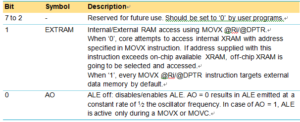
To access the expanded RAM, the EXTRAM bit must be cleared and MOVX instructions must be used. The extra 768 bytes of memory is physically located on the chip and logically occupies the first 768 bytes of external memory (addresses 000H to 2FFH).
When instructions access addresses in the upper 128 bytes (above 7FH), the MCU determines whether to access the SFRs or RAM by the type of instruction given. If it is indirect, then RAM is accessed through Crack NXP P87C552 Microcontroller Flash Memory. If it is direct, then an SFR is accessed. See the examples below.
Indirect Access: MOV@R0, #data; R0 contains 90H
Register R0 points to 90H which is located in the upper address range. Data in ‘#data’ is written to RAM location 90H rather than port 1.
Direct Access: MOV90H, #data; write data to P1
Data in ‘#data’ is written to port 1. Instructions that write directly to the address write to the SFRs.
To access the expanded RAM, the EXTRAM bit must be cleared and MOVX instructions must be used. The extra 768 bytes of memory is physically located on the chip and logically occupies the first 768 bytes of external memory (addresses 000H to 2FFH). see below picture:


