-
Product Categories
Live Support Chat


NXP Microcontroller P89LPC931 Firmware Unlocking
Manufacturer will normally choose to leave some backdoor port on the serial peripheral interface for NXP Microcontroller P89LPC931 Firmware Unlocking, hereby let’s introduce some of the features of it:
SPI features
• Master or slave operation
• 10 MHz bit frequency (max)
• LSB first or MSB first data transfer
• Four programmable bit rates
• End of transmission (SPIF)
• Write collision flag protection (WCOL)
• Wake-up from idle mode (slave mode only)
The serial peripheral interface (SPI) allows high-speed synchronous data transfer between the P89LPC931 and peripheral devices or between several P89LPC931 devices. Below Figure shows the correspondence between master and slave SPI devices.
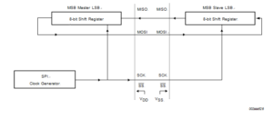
SPI master-slave interconnection
The SCK pin is the clock output and input for the master and slave modes, respectively. The SPI clock generator will start following a write to the master devices SPI data register. The written data is then shifted out of the MOSI pin on the master device into the MOSI pin of the slave device in order to complete the task of NXP MCU P87C554 Embedded Firmware Unlocking.
NXP Microcontroller P89LPC931 Firmware Unlocking
Following a complete transmission of one byte of data, the SPI clock generator is stopped and the SPIF flag is set. An SPI interrupt request will be generated if the SPI Interrupt Enable bit (SPIE) and the Serial Port Interrupt Enable bit (ES) are both set if NXP Microcontroller P89LPC931 Firmware Unlocking.
An external master drives the Slave Select input pin, SS/P1[4], low to select the SPI module as a slave. If SS/P1[4] has not been driven low, then the slave SPI unit is not active and the MOSI/P1[5] port can also be used as an input port pin. CPHA and CPOL control the phase and polarity of the SPI clock.