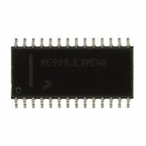
Motorola MC68HC908JK8 Embedded Flash Memory Restoration
Understand the operation of the embedded FLASH memory of Motorola MC68HC908JK8. This memory can be read, programmed, and erased from a single external supply. The program and erase operations are enabled through the use of an internal charge pump which can be taken advantage by Motorola MC68HC908JK8 Embedded Flash Memory Restoration process.
The FLASH memory is an array of 32,256 bytes with an additional 48 bytes of user vectors and one byte of block protection. An erased bit reads as logic 1 and a programmed bit reads as a logic 0. Memory in the FLASH array is organized into two rows per page basis. For the 32K word by 8-Bit Embedded FLASH Memory, the page size is 128 bytes per page.
Hence the minimum erase page size is 128 bytes. Program and erase operations are facilitated through control bits in the FLASH Control Register (FLCR). Details for these operations appear later in this section. The address ranges for the user memory and vectors are:
- $8000–$FDFF; user memory.
- $FF7E; FLASH block protect register.
- $FE08; FLASH control register.
- $FFDC–$FFFF; these locations are reserved for user-defined interrupt and reset vectors.
Programming tools are available from Freescale. Contact your local Freescale representative for more information.
NOTE: A security feature prevents viewing of the FLASH contents.
The FLASH control register (FLCR) controls FLASH program and erase operations.
HVEN — High-Voltage Enable Bit
This read/write bit enables the charge pump to drive high voltages for program and erase operations in the array to Unlock Motorola MC68HC908AZ60 Flash Heximal. HVEN can only be set if either PGM = 1 or ERASE = 1 and the proper sequence for program or erase is followed.
1 = High voltage enabled to array and charge pump on 0 = High voltage disabled to array and charge pump off


