Integrated Circuit Layout Design Function
The Integrated Circuit Layout Design Function is mainly reflected in the manufacturing process. The development process of semiconductor integrated circuits is a very complicated process. The main process steps are as follows:
(1) Design various functions and performances that the integrated circuit should have;
(2) Determine the electrical and physical properties required to achieve these functions and performance;
(3) Draw a logic diagram and circuit design diagram to achieve the above functions and performances;
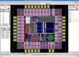
(4) rationally allocate the components required in the design circuit in each stack, and make the integrated circuit layout design of each laminate and the wiring and structural design of each component between each laminate;
(5) The IC layout design of each layer of the completed circuit three-dimensional layout is reduced and copied according to the physical requirements and design requirements, and the mask works for producing the chip are made. An integrated circuit having a set of mask works corresponding thereto;
(6) According to the mask work, adopt the relevant semiconductor process technology, and make the layout design of the circuit layer by layer on the semiconductor chip to form the chip;
(7) The chip is packaged to obtain an integrated circuit that can be used in practice.
In the above process, according to the integrated circuit layout design function and performance requirements, the layout design of the microscopic three-dimensional graphics formed by rationally distributing the required components in multiple layers of the integrated circuit is the key to the whole technology.
Because in the production process of integrated circuits, due to the high integration and interdependence of integrated circuits, plus the integrated circuit is made at one time, it is impossible to repair the wrong place or the unqualified place, as long as one of the integrated circuits Component errors, even a single connection error, are catastrophic and irreversible errors for integrated circuits.


