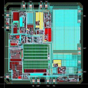
Integrated Circuit Layout Design Concept
Similar to integrated circuits, the definition of layout design differs in local legislation. The US law calls it a mask work; the Japanese law calls it a circuit layout; the EC directive calls it a topography; the World Intellectual Property Organization calls it a Layout design, China is consistent with the World Intellectual Property Organization, using the title of Integrated Circuit Layout Design.
Countries and regions not only have different names for layout designs, but also different expressions for definitions. The US Semiconductor Chip Protection Act states that a mask work refers to a series of images fixed or coded in any way.
They
(1) have or represent the presence of a coating on a semiconductor chip product, or from a semiconductor coating. A three-dimensional pattern of the removed metal material, insulating material or semiconductor material;
(2) In this series of images, the relationship between the images is that each image is a surface pattern of a structure of the semiconductor chip product.
The EC Directive on the Legal Protection of Semiconductor Product Topography states that a semiconductor product topology refers to a series of related images fixed or coded in any way:
(1) reflecting those constituting semiconductor products The three-dimensional configuration between the material layers;
(2) each image embodies the whole or part of the surface mode of each stage of the semiconductor product manufacturing process.
The WIPO Washington Treaty states that “layout design (topography)” refers to multiple components in an integrated circuit, at least one of which is an active component, and three or more of its integrated circuits are interconnected in three dimensions.
Configuration, or refers to such a three-dimensional configuration prepared for the fabrication of an integrated circuit. “Regulations on the Protection of Layout Design of Integrated Circuits” stipulates that the layout design of integrated circuits refers to the three-dimensional configuration of at least one of the integrated circuits and the interconnection of more than two components and some or all of the interconnected circuits, or for manufacturing integration. The above three-dimensional configuration prepared for the integrated circuit.


