Extract P89LPC917 Source Code
After the completion of Extract P89LPC917 Source Code, need to programme the source code to other blank P89LPC917, hereby we will discuss some details about programming:
A 50 % duty cycle clock can be programmed to come out on pin T2 (P1.0). This pin, besides being a regular I/O pin, has two additional functions. It can be programmed and MCU can be read:
1. To input the external clock for Timer/Counter 2, or
2. To output a 50 % duty cycle clock ranging from 122 Hz to 8 MHz at a 16 MHz operating frequency.
To configure the Timer/Counter 2 as a clock generator, bit C/T2 (in T2CON) must be cleared and bit T20E in T2MOD must be set. Bit TR2 (T2CON.2) also must be set to start the timer.
The Clock-Out frequency depends on the oscillator frequency and the reload value of Timer 2 capture registers (RCAP2H, RCAP2L) as shown in Equation 2:
OscillatorFrequency
—————————————————————————————–
2 65536 RCAP2H RCAP2L
Where (RCAP2H,RCAP2L) = the content of RCAP2H and RCAP2L taken as a 16-bit unsigned integer.
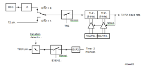
In the Clock-Out mode Timer 2 roll-overs will not generate an interrupt. This is similar to when it is used as a baud-rate generator to the purpose of NXP MCU P89LPC912 Binary Unlocking.
Bits TCLK and/or RCLK in T2CON allow the UART) transmit and receive baud rates to be derived from either Timer 1 or Timer 2. When TCLK = 0, Timer 1 is used as the UART transmit baud rate generator.
When TCLK = 1, Timer 2 is used as the UART transmit baud rate generator. RCLK has the same effect for the UART receive baud rate. With these two bits, the serial port can have different receive and transmit baud rates – Timer 1 or Timer 2.


