Dump MM908E624A Chip Memory Program
The EEPROM has a special security option, enabled by programming the EEPRTCT bit to 0 in the EEPROM non-volatile register (EENVR). Once security is enabled which will hinder Dump MM908E624A Chip Memory Program, the following limitations apply to the EEPROM:
• The 16-byte EEPROM locations from $08F0 to $08FF are protected from erase and program operations.
• The block erase and bulk erase modes are disabled. Byte erase can be used for all EEPROM locations except $08F0 to $08FF.
• The EENVR is protected from further erase or program operations.
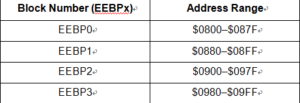
The 512 bytes of EEPROM is divided into four 128-byte blocks. Each of these blocks can be protected from erase/program operations by setting the EEBPx bit in the EENVR to facilitate the process of Decrypt P87LPC762 Locked Memory Program. Below Table shows the address ranges for the blocks.
These bits are effective after a reset or a read to EENVR register. The block protect configuration can be modified by erasing/programming the corresponding bits in the EENVR register and then reading the EENVR register.
The unprogrammed or erased state of an EEPROM bit is a logic 1. The factory default for the EEPROM array is $FF for all bytes.
The programming operation changes an EEPROM bit from logic 1 to logic 0 (programming cannot change a bit from logic 0 to a logic 1). In a single programming operation, the minimum EEPROM programming size is zero bits; the maximum is eight bits (one byte) from RECOVER MCU.
The erase operation changes an EEPROM bit from logic 0 to logic 1. In a single erase operation, the minimum EEPROM erase size is one byte; the maximum is the entire EEPROM array.
For each EEPROM byte, the write/erase endurance is 10,000 cycles. One write/erase cycle is defined as: a maximum of eight programming operations on the same byte followed by an erase operation of the that byte. Therefore, it is possible to program a byte, bit by bit to logic 0 before requiring an erase on that byte.


