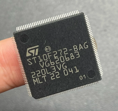
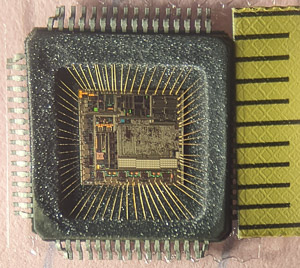
Dump Microprocessor ST10F272M-4T3 Protective Flash Memory Binary
Dump Microprocessor ST10F272M-4T3 Protective Flash Memory Binary needs to unlock ST10F272M mcu protection over its flash memory through reverse engineering encrypted microcontroller st10f272m firmware;

The XRAM is divided into two areas, the first 2 Kbytes named XRAM1 and the second 32 Kbytes named XRAM2, connected to the internal XBUS and are accessed like an external memory in 16-bit demultiplexed bus-mode without wait state or read/write delay (31.25ns access at 64 MHz CPU clock). Byte and Word accesses are allowed.

The XRAM1 address range is 00’E000h – 00’E7FFh if XPEN (bit 2 of SYSCON register), and XRAM1EN (bit 2 of XPERCON register) are set. If XRAM1EN or XPEN is cleared, then any access in the address range 00’E000h – 00’E7FFh will be directed to external memory interface, using the BUSCONx register corresponding to address matching ADDRSELx register.

The XRAM2 address range is F’0000h-F’7FFFFh if XPEN (bit 2 of SYSCON register), and XRAM2EN (bit 3 of XPERCON register) are set. If bit XPEN is cleared, then any access in the address range programmed for XRAM2 will be directed to external memory interface, using the BUSCONx register corresponding to address matching ADDRSELx register. The lower portion of the XRAM2 (address range F’0000h-F’3FFFFh) represents also the Stand-by RAM, which can be maintained biased through EA / VSTBY pin when main supply VDD is turned off.

