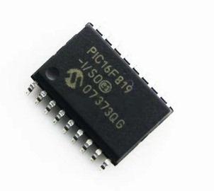
Discover Microchip MCU PIC16F819 Heximal
Discover Microchip MCU PIC16F819 Heximal which embed inside memory, copy locked heximal from microcontroller pic16f819 after reverse engineering microcontroller;

DEVICE OVERVIEW:
This document contains device specific information for the operation of the PIC16F819 devices. Additional information may be found in the “PICmicro® Mid-Range MCU Family Reference Manual” (DS33023) which may be downloaded from the Microchip web site. The Reference Manual should be considered a complementary document to this data sheet and is highly recommended reading for a better understanding of the device architecture and operation of the peripheral modules.
The PIC16F819 belongs to the Mid-Range family of the PICmicro® devices. The devices differ from each other in the amount of Flash program memory, data memory and data EEPROM (see Table 1-1). These devices contain features that are new to the PIC16 product line: which may be downloaded from the Microchip web site if extract avr atmel microcontroller secured memory.
The PIC16F819 devices have a 13-bit program counter capable of addressing an 8K x 14 program memory space. For the PIC16F819, the first 1K x 14 (0000h-03FFh) is physically implemented (see Figure 2-1). For the PIC16F819, the first 2K x 14 is located at 0000h-07FFh (see Figure 2-2). Accessing a location above the physically implemented address will cause a wraparound. For example, the same instruction will be accessed at locations 020h, 420h, 820h, C20h, 1020h, 1420h, 1820h and 1C20h when pull atmel avr mcu program.

The Reset vector is at 0000h and the interrupt vector is at 0004h.
The data memory is partitioned into multiple banks that contain the General Purpose Registers and the Special Function Registers. Bits RP1 (Status<6>) and RP0 (Status<5>) are the bank select bits.
Each bank extends up to 7Fh (128 bytes). The lower Locations of each bank are reserved for the Special Function Registers. Above the Special Function Registers are the General Purpose Registers, implemented as static RAM. All implemented banks contain SFRs. Some “high use” SFRs from one bank may be mirrored in another bank for code reduction and quicker access (e.g., the Status register is in Banks 0-3).

