Decode Renesas Microprocessor HD64F3644DV
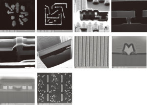
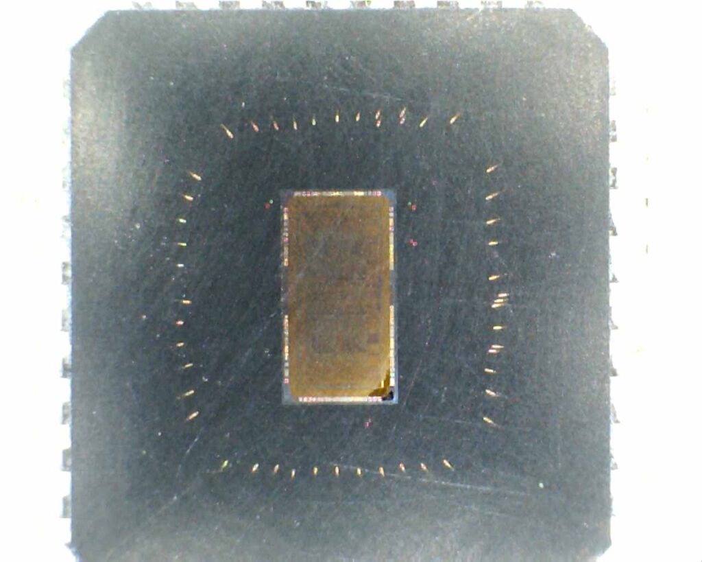
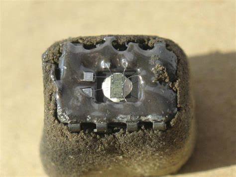
Decode Renesas Microprocessor HD64F3644DV flash memory and extract IC code out from its memory, semi-invasive cracking method will be applied which include the decapsulation, microprobing on the databus and then faulty injection inside the CPU and ADC/DAC counter;
The HD64F3644DV is a fast central processing unit with eight 16-bit general registers (also configurable as 16 eight-bit registers) and a concise instruction set designed for high-speed operation.
The main features of the HD64F3644DV CPU are listed below.
Two-way register configuration
¾ Sixteen 8-bit general registers, or ¾ Eight 16-bit general registers
Instruction set with 57 basic instructions, including:
¾ Multiply and divide instructions
¾ Powerful bit-manipulation instructions
Eight addressing modes
¾ Register direct (Rn)
¾ Register indirect (@Rn)
¾ Register indirect with displacement (@(d:16, Rn))
¾ Register indirect with post-increment or pre-decrement (@Rn+ or @–Rn)
¾ Absolute address (@aa:8 or @aa:16)
¾ Immediate (#xx:8 or #xx:16)
¾ PC-relative (@(d:8, PC))
¾ Memory indirect (@@aa:8)
Maximum 64-kbyte address space
High-speed operation
¾ All frequently-used instructions are executed in two to four states
Maximum clock rate (ø clock): 16 MHz at 5 V, 12 MHz at 4 V or 10 MHz at 3 V
¾ 8- or 16-bit register-register add or subtract: 125 ns (16 MHz), 167 ns (12 MHz), 200 ns (10 MHz)
¾ 8 ´ 8-bit multiply: 875 ns (16 MHz), 1167 ns (12 MHz), 1400 ns (10 MHz)
¾ 16 ¸ 8-bit divide: 875 ns (16 MHz), 1167 ns (12 MHz), 1400 ns (10 MHz)
Power-down mode
¾ SLEEP instruction
The HD64F3644DV CPU supports an address space with a maximum size of 64 kbytes for program code and data combined. The memory map differs depending on the mode (mode 1, 2, or 3) which can be applied over Crack HD64F3854HV Microprocessor Flash Program. For details, see section 3.4, Address Space Map in Each Operating Mode.
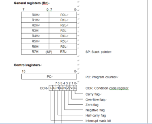
Below Figure shows the internal register structure of the HD64F3644DV CPU. There are two groups of registers: the general registers and control registers.
