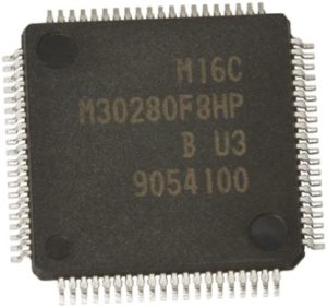
Decode MCU IC Renesas R5F212CCSNFP
Decode MCU IC Renesas R5F212CCSNFP
We can Decode MCU IC Renesas R5F212CCSNFP, please view the microcontroller chip features for your reference:
The R8C/2C Group and R8C/2D Group of single-chip MCUs incorporates the R8C/Tiny Series CPU core, employing sophisticated instructions for a high level of efficiency.
With 1 Mbyte of address space, and it is capable of executing instructions at high speed. In addition, the CPU core boasts a multiplier for high-speed operation processing.
Power consumption is low, and the supported operating modes allow additional power control. These MCUs also use an anti-noise configuration to reduce emissions of electromagnetic noise and are designed to withstand EMI.
Integration of many peripheral functions, including multifunction timer and serial interface, reduces the number of system components. Furthermore, the R8C/2D Group has on-chip data flash (1 KB × 2 blocks).
The difference between the R8C/2C Group and R8C/2D Group is only the presence or absence of data flash. Their peripheral functions are the same from Decode MCU IC Renesas R5F212CCSNFP.
|
CPU Central processing unit |
R8C/Tiny series core · Number of fundamental instructions: 89 · Minimum instruction execution time: 50 ns (f(XIN) = 20 MHz, VCC = 3.0 to 5.5 V) 100 ns (f(XIN) = 10 MHz, VCC = 2.7 to 5.5 V) 200 ns (f(XIN) = 5 MHz, VCC = 2.2 to 5.5 V) · Multiplier: 16 bits × 16 bits → 32 bits · Multiply-accumulate instruction: 16 bits × 16 bits + 32 bits → 32 bits · Operation mode: Single-chip mode (address space: 1 Mbyte) |
|
|
Memory ROM, RAM |
Refer to Table 1.5 Product List for R8C/2C Group. |
|
|
Power Supply Voltage detection Voltage circuit Detection |
· Power-on reset · Voltage detection 3 |
|
|
I/O Ports Programmable I/O ports |
· Input-only: 2 pins · CMOS I/O ports: 71, selectable pull-up resistor · High current drive ports: 8 |
|
|
Clock Clock generation circuits |
3 circuits: XIN clock oscillation circuit (with on-chip feedback resistor), On-chip oscillator (high-speed, low-speed) (high-speed on-chip oscillator has a frequency adjustment function), XCIN clock oscillation circuit (32 kHz) · Oscillation stop detection: XIN clock oscillation stop detection function · Frequency divider circuit: Dividing selectable 1, 2, 4, 8, and 16 · Low power consumption modes: Standard operating mode (high-speed clock, low-speed clock, high-speed on-chip oscillator, low-speed on-chip oscillator), wait mode, stop mode Real-time clock (timer RE) |
|
|
Interrupts |
· External: 5 sources, Internal: 23 sources, Software: 4 sources · Priority levels: 7 levels |
|
|
Watchdog Timer |
15 bits × 1 (with prescaler), reset start selectable |
|
|
Timer |
Timer RA |
8 bits × 1 (with 8-bit prescaler) Timer mode (period timer), pulse output mode (output level inverted every period), event counter mode, pulse width measurement mode, pulse period measurement mode |
| Timer RB |
8 bits × 1 (with 8-bit prescaler) Timer mode (period timer), programmable waveform generation mode (PWM output), programmable one-shot generation mode, programmable wait one- shot generation mode |
|
| Timer RC |
16 bits × 1 (with 4 capture/compare registers) Timer mode (input capture function, output compare function), PWM mode (output 3 pins), PWM2 mode (PWM output pin) |
|
| Timer RD |
16 bits × 2 (with 4 capture/compare registers) Timer mode (input capture function, output compare function), PWM mode (output 6 pins), reset synchronous PWM mode (output three-phase waveforms (6 pins), sawtooth wave modulation), complementary PWM mode (output three-phase waveforms (6 pins), triangular wave modulation), PWM3 mode (PWM output 2 pins with fixed period) |
|
| Timer RE |
8 bits × 1 Real-time clock mode (count seconds, minutes, hours, days of week), output compare mode |
|
| Timer RF |
16 bits × 1 (with capture/compare register pin and compare register pin) Input capture mode, output compare mode |
|
|
Item |
Function |
Specification |
|
Serial Interface |
UART0, UART1, UART2 |
Clock synchronous serial I/O/UART × 3 |
|
Clock Synchronous Serial I/O with Chip Select (SSU) |
2 1 (shared with I C-bus) |
|
|
2 (1) I C bus |
1 (shared with SSU) |
|
|
LIN Module |
Hardware LIN: 1 (timer RA, UART0) |
|
|
A/D Converter |
10-bit resolution × 20 channels, includes sample and hold function, with sweep mode |
|
|
D/A Converter |
8-bit resolution × 2 circuits |
|
|
Flash Memory |
· Programming and erasure voltage: VCC = 2.7 to 5.5 V · Programming and erasure endurance: 100 times · Program security: ROM code protect, ID code check · Debug functions: On-chip debug, on-board flash rewrite function |
|
|
Operating Frequency/Supply Voltage |
f(XIN) = 20 MHz (VCC = 3.0 to 5.5 V) f(XIN) = 10 MHz (VCC = 2.7 to 5.5 V) f(XIN) = 5 MHz (VCC = 2.2 to 5.5 V) |
|
|
Current consumption |
12 mA (VCC = 5.0 V, f(XIN) = 20 MHz) 5.5 mA (VCC = 3.0 V, f(XIN) = 10 MHz) 2.1 µA (VCC = 3.0 V, wait mode (f(XCIN) = 32 kHz)) 0.65 µA (VCC = 3.0 V, stop mode) |
|
|
Operating Ambient Temperature |
-20 to 85°C (N version) (2) -40 to 85°C (D version) (3) -20 to 105°C (Y version) |
|
|
Package |
80-pin LQFP Package code: PLQP0080KB-A (previous code: 80P6Q-A) |
|


