Decode Locked Philip P87C576 MCU Data
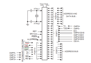
Pin definition on Philip P87C576 MCU can provide very important information for Decode Locked Philip P87C576 MCU Data, below we would like to introduce them:
Ground: 0V reference.
Power Supply: This is the power supply voltage for normal, idle, and power-down operation.
Port 0: Port 0 is an open-drain bidirectional I/O port. Port 0 pins that have 1s written to them float and can be used as high-impedance inputs. Port 0 is also the multiplexed low-order address and data bus during accesses to external program and data memory MCU reading. In this application, it uses strong internal pull-ups when emitting 1s. Port 0 also receives code bytes during EPROM programming and outputs code bytes during program verification.
External pull-ups are required during program verification. During reset, port 0 will be asynchronously driven low and will remain low until written to by software acquired from NXP P89C662 MCU Flash Memory cracking. All port 0 pins have Schmitt trigger inputs with 200mV hysteresis. A weak pulldown on port 0 guarantees positive leakage current (see DC Electrical Characteristics: IL1).
Port 1: Port 1 is an 8-bit bidirectional I/O port. Port 1 pins have internal pull-ups such that pins that have 1s written to them can be used as inputs but will source current when externally pulled low (see DC Electrical Characteristics: IIL).
Port 1 receives the low-order address byte during program memory verification and EPROM programming. During reset, port 1 will be asynchronously driven low and will remain low until written to by software from Decode Locked Philip P87C576 MCU Data. All port 1 pins have Schmitt trigger inputs with 50mV hysteresis. Port 1 pins also serve alternate functions as follows:
P1.0 T2 Timer 2 external I/O – clockout (programmable)
CMP0+ Comparator 0 positive input
P1.1 T2EX Timer 2 capture input
CMP0- Comparator 0 negative input
P1.2 ECI PCA count input
P1.3 CEX0 PCA module 0 external I/O
CMP0 Comparator 0 output
P1.4 CEX1 PCA module 1 external I/O
CMP1 Comparator 1 output
P1.5 CEX2 PCA module 2 external I/O
CMP2 Comparator 2 output
P1.6 CEX3 PCA module 3 external I/O
CMP3 Comparator 3 output
P1.7 CEX4 PCA module 4 external I/O
Port 2: Port 2 is an 8-bit bidirectional I/O port with internal pull-ups. Port 2 pins that have 1s written to them can be used as inputs, but will source current when externally pulled low (see DC Electrical Characteristics: IIL). Port 2 emits the high-order address byte during accesses to external program and data memory that use 16-bit addresses (MOVX @DPTR).
In this application, it uses strong internal pull-ups when emitting 1s. Port 2 receives the high-order address byte during program verification and EPROM programming. During reset, port 2 will be asynchronously driven low and will remain low until written to by software after NXP P87C453 Microcomputer Flash Code Cloning.
Port 2 can be made open drain by writing to the P2OD register (AIH). In open drain mode, weak pulldowns on port 2 guarantee positive leakage current (see DC Electrical Characteristics IL1).
Port 3: Port 3 is an 8-bit bidirectional I/O port with internal pull-ups. Port 3 pins except P3.1 that have 1s written to them can be used as inputs but will source current when externally pulled low (see DC Electrical Characteristics: IIL). P3.1 will be a high impedance pin except while transmitting serial data, in which case the strong pull-up will remain on continuously when outputting a 1 level.
The P3.1 output drive level when transmitting can be set to one of two levels by the writing to the P3.1 register bit. During reset all pins (except P3.1) will be asynchronously driven low and will remain low until written to by software.
All port 3 pins have Schmitt trigger inputs with 200mV hysteresis, except P3.2 and P3.3, which have 50mV
hysteresis. Port 3 pins serve alternate functions as follows:


