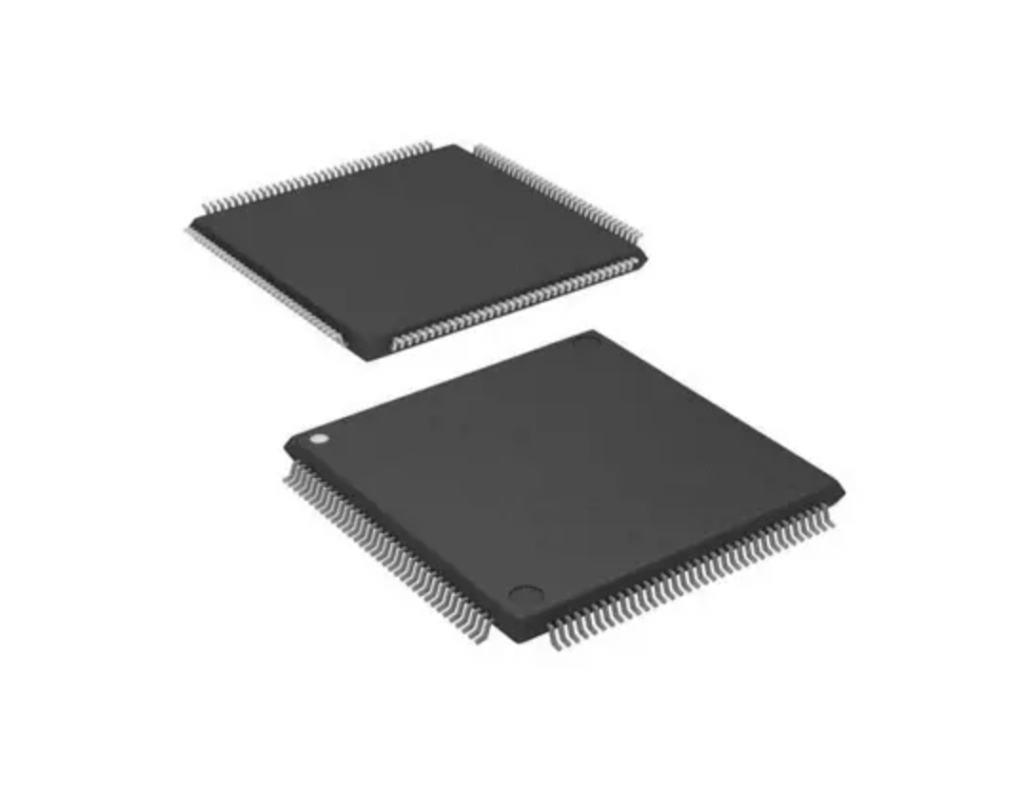
Crack ST10F271Z1T3 Secured Microcontroller Flash Memory
Crack ST10F271Z1T3 Secured Microcontroller Flash Memory and dump embedded firmware out from ST10F271Z1T3 microprocessor memory, clone heximal or binary program to new MCU ST10F271Z1T3;

EA pin assumes a new alternate functionality: it is also used to provide a dedicated power supply (see VSTBY) to maintain biased a portion of the XRAM (16 Kbytes) when the main Power Supply of the device (VDD and consequently the internally generated V18) is turned off for low power mode, allowing data retention. VSTBY voltage shall be in the range 4.5 to
5.5 volts and a dedicated embedded low power voltage regulator is in charge to provide the
1.8 V for the RAM, the low-voltage section of the 32 kHz oscillator and the Real Time Clock module when not disabled. It is allowed to exceed the upper limit up to 6 V for a very short period of time during the global life of the device and exceed the lower limit down to 4 V when RTC and 32 kHz on-chip oscillator are not used.
A second SSC mapped on the XBUS is added (SSC of ST10F271Z1T3 MCU becomes here SSC0, while the new one is referred as XSSC or simply SSC1). Note that some restrictions and functional differences due to the XBUS peculiarities are present between the classic SSC and the new XSSC. A second ASC mapped on the XBUS is added (ASC0 of ST10F269 remains ASC0, while the new one is referred as XASC or simply as ASC1).
Note that some restrictions and functional differences due to the XBUS peculiarities are present between the classic ASC and the new XASC. A second PWM mapped on the XBUS is added (PWM of ST10F271Z1T3 becomes here PWM0, while the new one is referred as XPWM or simply as PWM1). Note that some restrictions and functional differences due to the XBUS peculiarities are present between the classic PWM and the new XPWM.

