Crack PIC16LF627A Processor Data Eeprom
Crack PIC16LF627A processor data eeprom and dump embedded firmware from secured MICROCHIP MCU PIC16LF627A flash memory and eeprom memory, the original binary content or heximal source code can be restored from protective microprocessor PIC16LF627A;

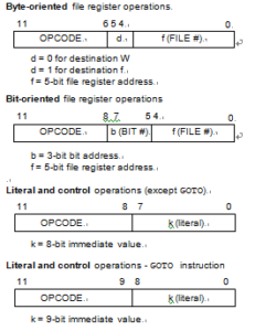
The destination designator specifies where the result of the operation is to be placed when Crack PIC16LF627A Processor Data Eeprom. If ‘d’ is ‘0’, the result is placed in the W register. If ‘d’ is ‘1’, the result is placed in the file register specified in the instruction.

For bit-oriented instructions, ‘b’ represents a bit field designator which selects the number of the bit affected by the operation of Break MC68HC908EY16 Microprocessor Protected Flash, while ‘f’ represents the number of the file in which the bit is located.
For literal and control operations, ‘k’ represents an 8 or 9-bit constant or literal value.
All instructions are executed within a single instruction cycle, unless a conditional test is true or the program counter is changed as a result of an instruction. In this case, the execution takes two instruction cycles in Break IC.

One instruction cycle consists of four oscillator periods. Thus, for an oscillator frequency of 4 MHz, the normal instruction execution time is 1 ms. If a conditional test is true or the program counter is changed as a result of an instruction acquired from Duplicate MCU PIC16C57 Memory Program, the instruction execution time is 2 ms.
Below Figure shows the three general formats that the instructions can have. All examples in the figure use the following format to represent a hexadecimal number:

0xhhh
where ‘h’ signifies a hexadecimal digit.

Note
1: The 9th bit of the program counter will be forced to a ‘0’ by any instruction that writes to the PC except for GOTO. (Section 4.6)
2: When an I/O register is modified as a function of itself from Crack IC dsPIC30F6012A Software (e.g. MOVF PORTB, 1), the value used will be that value present on the pins themselves after Crack PIC16LF627A Processor Data Eeprom. For example, if the data latch is ‘1’ for a pin configured as input and is driven low by an external device, the data will be written back with a ‘0’.
3: The instruction TRIS f, where f = 6 causes the contents of the W register to be written to the tristate latches of PORTB. A ‘1’ forces the pin to a hi-impedance state and disables the output buffers which will support the process of Unlock Microchip PIC12LC508A Memory Program.

4: If this instruction is executed on the TMR0 register (and, where applicable, d = 1), the prescaler will be cleared (if assigned to TMR0).

