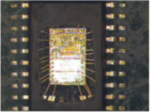
Crack Philip P87C652 Microcontroller Protected Memory
Understand the pin definition of P87C652 can help us to have a better idea about the cracking procedures, hereby we would like to to introduce P87C652 with various footprint for your reference related to Crack Philip P87C652 Microcontroller Protected Memory:
Reset: A low on this pin asynchronously resets all port pins to a low state except P3.1. The pin must be held low with the oscillator running for 24 oscillator cycles to initialize the internal registers. An internal diffused resistor to VCC permits a power on reset using only an external capacitor to VSS.
RST has a Schmitt trigger input stage to provide additional noise immunity with a slow rising input voltage. Address Latch Enable/Program Pulse: Output pulse for latching the low byte of the address during an access to external memory by MCU reading. In normal operation, ALE is emitted at a constant rate of 1/6 the oscillator frequency, and can be used for external timing or clocking after Crack Philip P87C652 Microcontroller Protected Memory.
Note that one ALE pulse is skipped during each access to external data memory. ALE is switched off if the bit 0 in the AUXR register (8EH) is set. This pin is also the program pulse input (PROG) during EPROM programming. Program Store Enable: The read strobe to external program memory.
When the device is executing code from the external program memory, PSEN is activated twice each machine cycle, except that two PSEN activations are skipped during each access to external data memory. PSEN is not activated during fetches from internal program memory.
External Access Enable/Programming Supply Voltage: EA must be externally held low to enable the device to fetch code from external program memory locations 0000H to 1FFFH. If EA is held high, the device executes from internal program memory unless the program counter contains an address greater than 1FFFH only after the progress of NXP P89C662 MCU Flash Memory cracking has been completed.
This pin also receives the 12.75V programming supply voltage (VPP) during EPROM programming. Crystal 1: Input to the inverting oscillator amplifier and input to the internal clock generator circuits.
Crystal 2: Output from the inverting oscillator amplifier.


