Crack Microcontroller AT89C51CC03 Binary
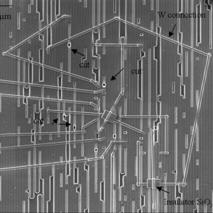
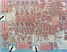
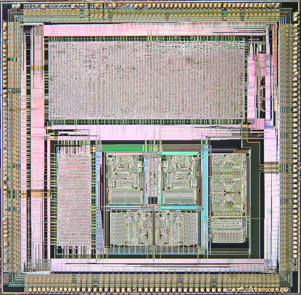
Crack Microcontroller AT89C51CC03 tamper defending mechanism and extract binary from MCU AT89C51CC03 include flash and eeprom memory, to make processor AT89C51CC03 recovery;
It is not obvious the last three instructions in this list are Read-Modify-Write instructions. These instructions read the port (all 8 bits), modify the specifically addressed bit and write the new byte back to the latch.
These Read-Modify-Write instructions are directed to the latch rather than the pin in order to avoid possible misinterpretation of voltage (and therefore, logic) levels at the pin. For example, a Port bit used to drive the base of an external bipolar transistor can not rise above the transistor’s base-emitter junction voltage (a value lower than VIL) if Crack Mcu pic16c63a heximal.
With a logic one written to the bit, attempts by the CPU to read the Port at the pin are misinterpreted as logic zero. A read of the latch rather than the pins returns the correct logic-one value.
Port 1, Port 2, Port 3 and Port 4 have fixed internal pull-ups and are referred to as “quasi-bidirectional” Ports. When configured as an input, the pin impedance appears as logic one and sources current in response to an external logic zero condition. Port 0 is a “true bidirectional” pin. The pins float when configured as input. Resets write logic one to all Port latches. If logical zero is subsequently written to a Port latch, it can be returned to input conditions by a logical one written to the latch after Crack chip pic16c73b firmware.
Port latch values change near the end of Read-Modify-Write instruction cycles. Output buffers (and therefore the pin state) update early in the instruction after Read-Modify-Write instruction cycle.
Logical zero-to-one transitions in Port 1, Port 2, Port 3 and Port 4 use an additional pull-up (p1) to aid this logic transition (see Figure 4.). This increases switch speed. This extra pull-up sources 100 times normal internal circuit current during 2 oscillator clock periods.
The internal pull-ups are field-effect transistors rather than linear resistors. Pull-ups consist of three p-channel FET (pFET) devices. A pFET is on when the gate senses logical zero and off when the gate senses logical one. pFET #1 is turned on for two oscillator periods immediately after a zero-to-one transition in the Port latch.
A logical one at the Port pin turns on pFET #3 (a weak pull-up) through the inverter. This inverter and pFET pair form a latch to drive logical one. pFET #2 is a very weak pull-up switched on whenever the associated nFET is switched off. This is traditional CMOS switch convention. Current strengths are 1/10 that of pFET #3.
Tags: crack microcontroller binary archive,crack microcontroller binary code,crack microcontroller binary content,crack microcontroller binary data,crack microcontroller binary eeprom,crack microcontroller binary file,crack microcontroller binary firmware,crack microcontroller binary information,crack microcontroller binary memory,crack microcontroller binary program


