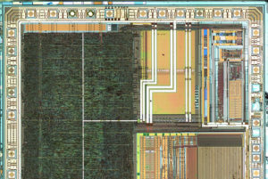
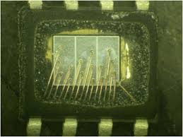
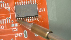
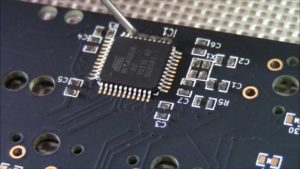
Crack MCU PIC18F4510 Firmware
Crack MCU PIC18F4510 is for the purpose of Firmware extracting from the microcontroller memory include flash and eeprom, the reading out process needs to unlock microcontroller before proceeding, and the copied code will be exactly the same as original version;
Crack MCU PIC18F4510 is for the purpose of Firmware extracting from the microcontroller memory include flash and eeprom, the reading out process needs to unlock microcontroller before proceeding, and the copied code will be exactly the same as original version;
Using the internal oscillator as the clock source eliminates the need for up to two external oscillator pins, which can then be used for digital I/O. Two distinct configurations are available:
· In INTIO1 mode, the OSC2 pin outputs FOSC/4, while OSC1 functions as RA7 for digital input and output.
· In INTIO2 mode, OSC1 functions as RA7 and OSC2 functions as RA6, both for digital input and output.
The internal oscillator block is calibrated at the factory to produce an INTOSC output frequency of 8.0 MHz.
The INTRC oscillator operates independently of the INTOSC source. Any changes in INTOSC across voltage and temperature are not necessarily reflected by changes in INTRC and vice versa.
The internal oscillator’s output has been calibrated at the factory but can be adjusted in the user’s application to faciliate the process of MCU program reading. This is done by writing to the OSCTUNE register (Register 2-1). The tuning sensitivity is constant throughout the tuning range.
When the OSCTUNE register is modified, the INTOSC frequency will begin shifting to the new frequency. The INTRC clock will reach the new frequency within 8 clock cycles (approximately 8 * 32 µs = 256 µs). The INTOSC clock will stabilize within 1 ms. Code execution continues during this shift. There is no indication that the shift has occurred.
The OSCTUNE register also implements the INTSRC and PLLEN bits, which control certain features of the internal oscillator block. The INTSRC bit allows users to select which internal oscillator provides the clock source when the 31 kHz frequency option is selected.
This is covered in greater detail in Section 2.7.1
“Oscillator Control Register”.
The PLLEN bit controls the operation of the frequency multiplier, PLL, in internal oscillator modes.
The 4x frequency multiplier can be used with the internal oscillator block to produce faster device clock speeds than are normally possible with an internal oscillator. When enabled, the PLL produces a clock speed of up to 32 MHz.
Unlike HSPLL mode, the PLL is controlled through software. The control bit, PLLEN (OSCTUNE<6>), is used to enable or disable its operation.
The PLL is available when the device is configured to use the internal oscillator block as its primary clock source (FOSC3:FOSC0 = 1001 or 1000). Additionally, the PLL will only function when the selected output frequency is either 4 MHz or 8 MHz (OSCCON<6:4> =111 or 110). If both of these conditions are not met, the PLL is disabled.
The PLLEN control bit is only functional in those internal oscillator modes where the PLL is available. In all other modes, it is forced to ‘0’ and is effectively unavailable.The factory calibrates the internal oscillator block output (INTOSC) for 8 MHz.
However, this frequency may drift as VDD or temperature changes, which can affect the controller operation in a variety of ways. It is possible to adjust the INTOSC frequency by modifying the value in the OSCTUNE register. This has no effect on the INTRC clock source frequency.
Tuning the INTOSC source requires knowing when to make the adjustment, in which direction it should be made and in some cases, how large a change is needed.
Tags: crack mcu embedded archive,crack mcu embedded code,crack mcu embedded content,crack mcu embedded data,crack mcu embedded eeprom,crack mcu embedded file,crack mcu embedded firmware,crack mcu embedded information,crack mcu embedded memory,crack mcu embedded program


