Crack MCU PIC16F721 Binary
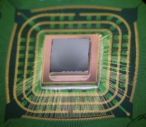
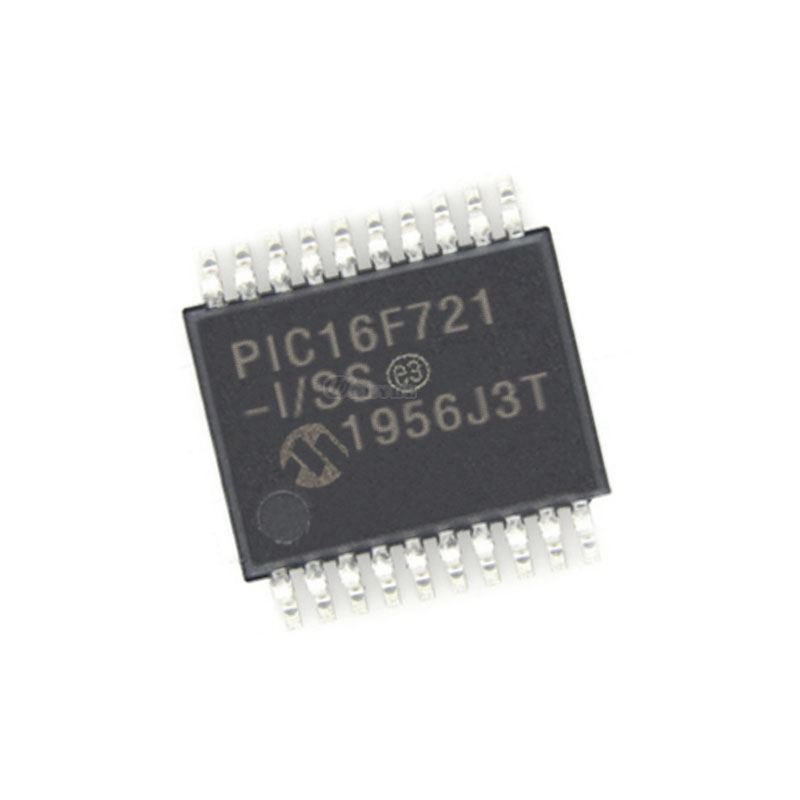
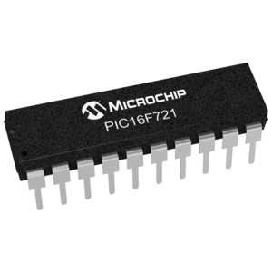
Crack MCU PIC16F721 and then copy microprocessor pic16f721 secured memory binary, reverse engineering microcontroller pic16f721 internal structure to analyze the location of its flash memory and eeprom memory;

Master mode of operation is supported in firmware using interrupt generation on the detection of the Start and Stop conditions. The Stop (P) and Start (S) bits of the SSPSTAT register are cleared from a Reset or when the SSP module is disabled (SSPEN cleared).
The Stop (P) and Start (S) bits will toggle based on the Start and Stop conditions. Control of the I2C bus may be taken when the P bit is set or the bus is Idle and both the S and P bits are clear. In Firmware Master mode, the SCL and SDA lines are manipulated by setting/clearing the corresponding TRIS bit(s). The output level is always low, irrespective of the value(s) in the corresponding PORT register bit(s) if Crack pic16f873 MCU.
When transmitting a ‘1’, the TRIS bit must be set (input) and a ‘0’, the TRIS bit must be clear (output). The following events will cause the SSP Interrupt Flag bit, SSPIF, to be set (SSP Interrupt will occur if enabled):
· Start condition
· Stop condition
· Data transfer byte transmitted/received
Firmware Master mode of operation can be done with either the Slave mode Idle (SSPM<3:0> = 1011), or with either of the Slave modes in which interrupts are enabled. When both master and slave functionality is enabled, the software needs to differentiate the source(s) of the interrupt.
In Multi-Master mode, the interrupt generation on the detection of the Start and Stop conditions allow the determination of when the bus is free. The Stop (P) and Start (S) bits are cleared from a Reset or when the SSP module is disabled. The Stop (P) and Start (S) bits will toggle based on the Start and Stop conditions before break avr attiny2313 MCU.
Control of the I2C bus may be taken when the P bit of the SSPSTAT register is set or when the bus is Idle, and both the S and P bits are clear. When the bus is busy, enabling the SSP Interrupt will generate the interrupt when the Stop condition occurs.
In Multi-Master operation, the SDA line must be monitored to see if the signal level is the expected output level. This check only needs to be done when a high level is output. If a high level is expected and a low level is present, the device needs to release the SDA and SCL lines (set TRIS bits). There are two stages where this arbitration of the bus can be lost. They are the Address Transfer and Data Transfer stages.
When the slave logic is enabled, the slave continues to receive. If arbitration was lost during the address transfer stage, communication to the device may be in progress. If addressed, an ACK pulse will be generated. If arbitration was lost during the data transfer stage, the device will need to re-transfer the data at a later time.
Refer to Application Note AN578, “Use of the SSP Module in the I2C™ Multi-Master Environment” (DS00578) for more information. When the CKP bit is cleared, the SCL output is held low once it is sampled low. Therefore, the CKP bit will not stretch the SCL line until an external I2C master device has already asserted the SCL line low.
The SCL output will remain low until the CKP bit is set and all other devices on the I2C bus have released SCL. This ensures that a write to the CKP bit will not violate the minimum high time requirement for SCL When the device is code-protected, the CPU may continue to read and write the Flash program memory.
Depending on the settings of the Flash program memory enable (WRT<1:0>) bits, the device may or may not be able to write certain blocks of the program memory. However, reads of the program memory are allowed.

When the Flash program memory Code Protection (CP) bit in the Configuration Word register is enabled, the program memory is code-protected, and the device programmer (ICSP™) cannot access data or program memory. PMCON1 is the control register for the data program memory accesses.
Control bits RD and WR initiate read and write, respectively. These bits cannot be cleared, but only set in software. They are cleared in hardware at the completion of the read or write operation. The inability to clear the WR bit in software prevents the accidental premature termination of a write operation.

Setting the control bit WR initiates a write operation. For program memory writes, WR initiates a write cycle if FREE = 0 and an erase cycle if FREE = 1. The WREN bit, when set, will allow a write operation. On power-up, the WREN bit is clear. PMCON2 is not a physical register. Reading PMCON2 will read all ‘0’s. The PMCON2 register is used exclusively in the Flash memory write sequence.
Tags: megszakítja az MCU PIC16F721 flash memóriát,oldja fel az MCU PIC16F721 flash memóriát,repedés MCU PIC16F721 flash memória,támadás MCU PIC16F721 flash memória

