Crack MCU AT89C51AC3 Heximal
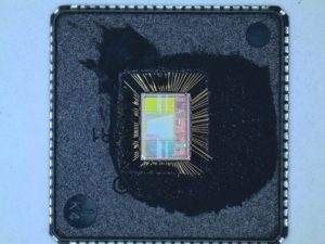
Crack MCU AT89C51AC3 program memory and data memory, read Heximal out from microcontroller AT89C51AC3 and download the firmware to new microprocessor AT89C51AC3 for MCU recovery;
Each Port SFR operates via type-D latches, as illustrated in Figure 1 for Ports 3 and 4. A CPU “write to latch” signal initiates transfer of internal bus data into the type-D latch. A CPU “read latch” signal transfers the latched Q output onto the internal bus.
Similarly, a “read pin” signal transfers the logical level of the Port pin. Some Port data instructions activate the “read latch” signal while others activate the “read pin” signal. Latch instructions are referred to as Read-Modify-Write instructions before unlock microcontroller pic10f220 hex.
Each I/O line may be independently programmed as input or output. Figure 1 shows the structure of Ports 1 and 3, which have internal pull-ups. An external source can pull the pin low. Each Port pin can be configured either for general-purpose I/O or for its alternate input output function.
To use a pin for general-purpose output, set or clear the corresponding bit in the Px register (x = 1,3 or 4). To use a pin for general-purpose input, set the bit in the Px register. This turns off the output FET drive after Crack MCU dsPIC30F1010 heximal.
To configure a pin for its alternate function, set the bit in the Px register. When the latch is set, the “alternate output function” signal controls the output level (see Figure 1). The operation of Ports 1, 3 and 4 is discussed further in the “quasi-Bidirectional Port Operation” section.
Ports 0 and 2 are used for general-purpose I/O or as the external address/data bus. Port 0, shown in Figure 3, differs from the other Ports in not having internal pull-ups. Figure 3 shows the structure of Port 2. An external source can pull a Port 2 pin low before Crack Microcontroller dsPIC30F2023 eeprom.
To use a pin for general-purpose output, set or clear the corresponding bit in the Px register (x = 0 or 2). To use a pin for general-purpose input, set the bit in the Px register to turn off the output driver FET.
Some instructions read the latch data rather than the pin data. The latch based instructions read the data, modify the data and then rewrite the latch. These are called “Read-Modify-Write” instructions. Below is a complete list of these special instructions (see Table ). When the destination operand is a Port or a Port bit, these instructions read the latch rather than the pin when Crack MCU.
Tags: crack mcu binary archive,crack mcu binary code,crack mcu binary content,crack mcu binary data,crack mcu binary eeprom,crack mcu binary file,crack mcu binary firmware,crack mcu binary information,crack mcu binary memory,crack mcu binary program


