Crack IC AT89C5115 Code
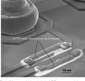
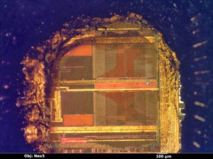
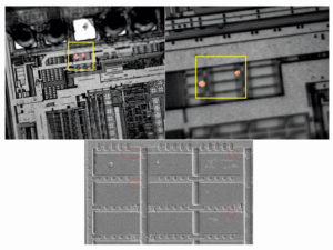
Crack IC AT89C5115 and break Microcontroller security fuse bit by focus ion beam and extract embedded Code from MCU flash memory;
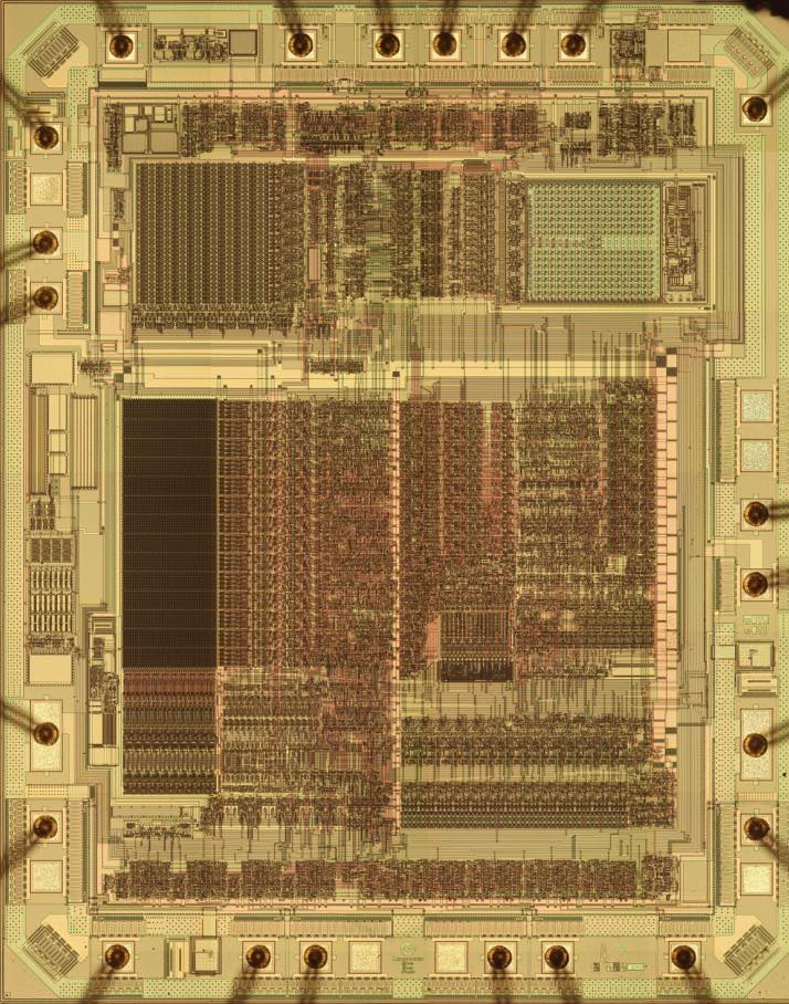
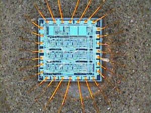
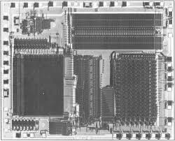
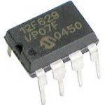
The T89C5115 is a high performance Flash version of the 80C51 single chip 8-bit microcontrollers. It contains a 16-KB Flash memory block for program and data. The 16-KB Flash memory can be programmed either in parallel mode or in serial mode with the ISP capability or with software. The programming voltage is internally generated from the standard VCC pin.
The T89C5115 retains all features of the 80C52 with 256 bytes of internal RAM, a 7 source 4-level interrupt controller and three timer/counters. In addition, the T89C5115 has a 10-bit A/D converter, a 2-KB Boot Flash memory, 2-KB EEPROM for data, a Programmable Counter Array, an XRAM of 256 bytes, a Hardware WatchDog Timer and a more versatile serial channel that facilitates multiprocessor communication (EUART) if unlock microcontroller at89c51rc2 eeprom.
The fully static design of the T89C5115 reduces system power consumption by bringing the clock frequency down to any value, even DC, without loss of data. The T89C5115 has two software-selectable modes of reduced activity and an 8 bit clock prescaler for further reduction in power consumption. In the idle mode the CPU is frozen while the peripherals and the interrupt system are still operating. In the power-down mode the RAM is saved and all other functions are inoperative.
The added features of the T89C5115 make it more powerful for applications that need A/D conversion, pulse width modulation, high speed I/O and counting capabilities such as industrial control, consumer goods, alarms, motor control, etc. While remaining fully compatible with the 80C52 it offers a superset of this standard microcontroller.
In X2 mode a maximum external clock rate of 20 MHz reaches a 300 ns cycle time.
Port Structure
Each Port SFR operates via type-D latches, as illustrated in Figure 1 for Ports 3 and 4. A CPU ’write to latch’ signal initiates transfer of internal bus data into the type-D latch. A CPU ’read latch’ signal transfers the latched Q output onto the internal bus. Similarly, a ’read pin’ signal transfers the logical level of the Port pin. Some Port data instructions activate the ’read latch’ signal while others activate the ’read pin’ signal if unlock mcu at89c51ed2 flash.
Latch instructions are referred to as Read-Modify-Write instructions. Each I/O line may be independently programmed as input or output. Figure 1 shows the structure of Ports, which have internal pull-ups. An external source can pull the pin low. Each Port pin can be configured either for general-purpose I/O or for its alternate input output function.
To use a pin for general-purpose output, set or clear the corresponding bit in the Px register (x = 1 to 4). To use a pin for general-purpose input, set the bit in the Px register. This turns off the output FET drive. To configure a pin for its alternate function, set the bit in the Px register. When the latch is set, the ’alternate output function’ signal controls the output level (See Figure 1). The operation of Ports is discussed further in ’Quasi-Bi-directional Port Operation’ paragraph.
It is not obvious that the last three instructions in this list are Read-Modify-Write instructions. These instructions read the port (all 8 bits), modify the specifically addressed bit and write the new byte back to the latch. These Read-Modify-Write instructions are directed to the latch rather than the pin in order to avoid possible misinterpretation of voltage (and therefore, logic) levels at the pin.
For example, a Port bit used to drive the base of an external bipolar transistor cannot rise above the transistor’s base-emitter junction voltage (a value lower than VIL). With a logic one written to the bit, attempts by the CPU to read the Port at the pin are misinterpreted as logic zero. A read of the latch rather than the pins returns the correct logic one value.
Tags: crack ic heximal archive,crack ic heximal code,crack ic heximal content,crack ic heximal data,crack ic heximal eeprom,crack ic heximal file,crack ic heximal firmware,crack ic heximal information,crack ic heximal memory,crack ic heximal program


