Crack Chip dsPIC30F3013 Eeprom
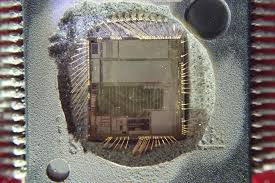
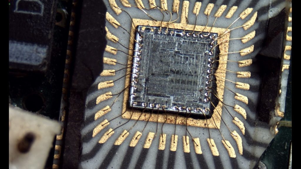
Crack Chip dsPIC30F3013 and readout the program from MCU dsPIC30F3013 flash memory, the whole functions of microcontroller can be recovered through this process;
W15 is initialized to 0x0800 during a Reset. The user may reprogram the SP during initialization to any location within data space.W14 has been dedicated as a stack frame pointer as defined by the LNK and ULNK instructions. However, W14 can be referenced by any instruction in the same manner as all other W registers.
The dsPIC core has a 16-bit STATUS register (SR), the LS Byte of which is referred to as the SR Low byte (SRL) and the MS Byte as the SR High byte (SRH). See Figure 2-1 for SR layout. SRL contains all the MCU ALU operation status flags (including the Z bit), as well as the CPU Interrupt Priority Level status bits, IPL<2:0> and the Repeat Active status bit, RA. During exception processing, SRL is concatenated with the MS Byte of the PC to form a complete word value which is then stacked if clone ic microchip dspic30f3010 program.
The upper byte of the STATUS register contains the DSP Adder/Subtracter status bits, the DO Loop Active bit (DA) and the Digit Carry (DC) status bit. The program counter is 23-bits wide; bit 0 is always clear. Therefore, the PC can address up to 4M instruction words.
The dsPIC devices feature a 16/16-bit signed fractional divide operation, as well as 32/16-bit and 16/16-bit signed and unsigned integer divide operations, in the form of single instruction iterative divides. The following instructions and data sizes are supported:
DIVF – 16/16 signed fractional divide
DIV.sd – 32/16 signed divide
DIV.ud – 32/16 unsigned divide
DIV.sw – 16/16 signed divide
5. DIV.uw – 16/16 unsigned divide
The 16/16 divides are similar to the 32/16 (same number of iterations), but the dividend is either zero-extended or sign-extended during the first iteration. The divide instructions must be executed within a REPEAT loop. Any other form of execution (e.g., a series of discrete divide instructions) will not function correctly because the instruction flow depends on RCOUNT if retrieve microcomputer pic18f2550.
The divide instruction does not automatically set up the RCOUNT value and it must, therefore, be explicitly and correctly specified in the REPEAT instruction as shown in Table 2-1 (REPEAT will execute the target instruction {operand value+1} times). The REPEAT loop count must be setup for 18 iterations of the DIV/DIVF instruction. Thus, a complete divide operation requires 19 cycles.
The DSP engine consists of a high speed 17-bit x 17-bit multiplier, a barrel shifter and a 40-bit adder/subtracter (with two target accumulators, round and saturation logic). The DSP engine also has the capability to perform inherent accumulator-to-accumulator operations, which require no additional data. These instructions are ADD, SUB and NEG.
The dsPIC30F is a single-cycle instruction flow architecture, threfore, concurrent operation of the DSP engine with MCU instruction flow is not possible. However, some MCU ALU and DSP engine resources may be used concurrently by the same instruction (e.g., ED, EDAC).
The 17 x 17-bit multiplier is capable of signed or unsigned operation and can multiplex its output using a scaler to support either 1.31 fractional (Q31) or 32-bit integer results. Unsigned operands are zero-extended into the 17th bit of the multiplier input value. Signed operands are sign-extended into the 17th bit of the multiplier input value.
The output of the 17 x 17-bit multiplier/scaler is a 33-bit value which is sign-extended to 40 bits. Integer data is inherently represented as a signed two’s complement value, where the MSB is defined as a sign bit. Generally speaking, the range of an N-bit two’s complement integer is -2N-1 to 2N-1 – 1.
For a 16-bit integer, the data range is -32768 (0x8000) to 32767 (0x7FFF) including ‘0’. For a 32-bit integer, the data range is -2,147,483,648 (0x8000 0000) to 2,147,483,645 (0x7FFF FFFF). When the multiplier is configured for fractional multiplication, the data is represented as a two’s complement fraction, where the MSB is defined as a sign bit and the radix point is implied to lie just after the sign bit (QX format).
The range of an N-bit two’s complement fraction with this implied radix point is -1.0 to (1 – 21-N). For a 16-bit fraction, the Q15 data range is -1.0 (0x8000) to 0.999969482 (0x7FFF) including ‘0’ and has a precision of 3.01518×10⁻⁵. In Fractional mode, the 16×16 multiply operation generates a 1.31 product which has a precision of 4.65661 x 10⁻¹⁰.
The same multiplier is used to support the MCU multiply instructions which include integer 16-bit signed, unsigned and mixed sign multiplies. The MUL instruction may be directed to use byte or word sized operands. Byte operands will direct a 16-bit result, and word operands will direct a 32-bit result to the specified register(s) in the W array.
Tags: crack chip binary archive,crack chip binary code,crack chip binary content,crack chip binary data,crack chip binary eeprom,crack chip binary file,crack chip binary firmware,crack chip binary information,crack chip binary memory,crack chip binary program


