-
Product Categories
Live Support Chat


CPLD Characteristic & Application
Complex Programmable Logic Device has the characteristics of flexible programming, high integration, short design and development period, wide application range, advanced development tools, low design and manufacturing cost, low hardware experience for designers, no need for testing of standard products, strong confidentiality and popular price.
It can realize large-scale circuit design, so it is widely used in product prototype design and product production (generally less than 10,000 pieces). CPLD devices can be used in almost all applications where small-scale general-purpose digital integrated circuits are used. CPLD devices have become an indispensable part of electronic products, and its design and application have become a must-have skill for electronics engineers.
A CPLD is a digital integrated circuit that users construct their own logic functions according to their needs. The basic design method is to use the integrated development software platform, use the schematic diagram, hardware description language and other methods to generate the corresponding target file, and transfer the code to the target chip through the download cable (“in-system” programming) to realize the designed digital system.
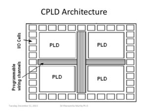
Complex Programmable Logic Device Architecture
Here, take the answering device as an example to talk about its design (renovation) process, that is, the design process of the chip. Most of the work of CPLD is done on a computer. Open the integrated development software (Altera Max+pluxII) → draw the schematic, write the hardware description language (VHDL, Verilog) → compile → give the input excitation signal of the logic circuit, perform simulation, check whether the logic output result is correct → carry out the pin Input and output lock (64 input and output pins of 7128 can be set as needed) → Generate code → Transfer and store the code in the CPLD chip through the download cable.
7128 The chip has been led out, the digital tube, the answering switch, the indicator light, the buzzer are respectively connected to the chip board through the wire, and the power is tested. When the answering switch is pressed, the corresponding indicator light should be on, correct. Later, after the referee gives extra points, see if the digital display bonus points are correct.
cpld application
If there is any problem, you can re-edit the schematic or hardware description language and improve the design. After designing, such as mass production, you can directly copy other CPLD chips, that is, write code and this technique has been widely used in Reverse PLD IC Altera EPM7064LC44-15. If you want to make other designs on the chip, such as traffic light design, re-draw the schematic, or write the hardware description language, repeat the above work process and complete the design. This modified design is equivalent to the renovation of the house, which can be performed tens of thousands of times for the CPLD.