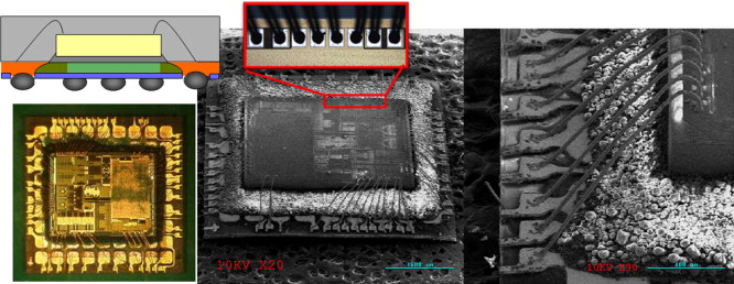
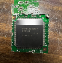
Clone Secured Renesas Microcontroller R5F56104VNFP#V0
Clone Secured Renesas Microcontroller R5F56104VNFP#V0 memory file which will provide the same functions as originals when break MCU security fuse bit and readout the firmware from microprocessor program;

- The subsequent instruction must be executed while an interrupt request is disabled with the IENj bit in IERn of the ICU (interrupt request enable bit) set to 0.
- A WAIT instruction is executed immediately after the preprocessing for causing a transition to the low power consumption state.
In the above cases, after writing to an I/O register, wait until the write operation is completed using the following procedure and then execute the subsequent instruction.
Write to an I/O register.

Read the value in the I/O register and write it to a general register.
Execute the operation using the value read.
Execute the subsequent instruction.
When executing an instruction after writing to multiple registers, only read the last I/O register written to and execute the instruction using that value; it is not necessary to execute the instruction using the values written to all the registers when cloning renesas mcu r5f21237 flash program.
- Number of cycles necessary for accessing I/O registers
See Table 4.1 for details on the number of clock cycles necessary for accessing I/O registers. The number of access cycles to I/O registers is obtained by following equation.*1

Number of access cycles to I/O registers = Number of bus cycles for internal main bus 1 + Number of divided clock synchronization cycles + Number of bus cycles for internal peripheral buses 1 to 6

