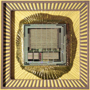
Clone Processor ATmega128V Code
Clone Processor ATmega128V Code is only a process to extract mcu atmega128v flash software, furthermore we have to decrypt the embedded firmware of microcontroller atmega128v to remove the encryption of heximal;

If desired, ALE operation can be disabled by setting bit 0 of SFR location 8EH. With the bit set, ALE is active only during a MOVX or MOVC instruction. Otherwise, the pin is weakly pulled high. Setting the ALE-disable bit has no effect if the microcontroller is in external execution mode.
PSEN
Program Store Enable is the read strobe to external program memory. When the AT89S53 is executing code from external program memory, PSEN is activated twice each machine cycle, except that two PSEN activations are skipped during each access to external data memory before crack mcu atmega640v hex.
EA/VPP
External Access Enable. EA must be strapped to GND in order to enable the device to fetch code from external program memory locations starting at 0000H up to FFFFH. Note, however, that if lock bit 1 is programmed, EA will be internally latched on reset.
EA should be strapped to VCC for internal program executions. This pin also receives the 12-volt programming enable voltage (VPP) during Flash programming when 12-volt programming is selected after crack mcu atmega1280v hex.
A map of the on-chip memory area called the Special Function Register (SFR) space is shown in Table 1. Note that not all of the addresses are occupied, and unoccupied addresses may not be implemented on the chip.
Read accesses to these addresses will in general return random data, and write accesses will have an indeterminate effect. User software should not write 1s to these unlisted locations, since they may be used in future products to invoke new features. In that case, the reset or inactive values of the new bits will always be 0.
Timer 2 Registers Control and status bits are contained in registers T2CON (shown in Table 2) and T2MOD (shown in Table 9) for Timer 2. The register pair (RCAP2H, RCAP2L) are the Capture/Reload registers for Timer 2 in 16 bit capture mode or 16-bit auto-reload mode.
Watchdog Control Register The WCON register contains control bits for the Watchdog Timer (shown in Table 3). The DPS bit selects one of two DPTR registers available.
Tags: clone processor archive,clone processor binary,clone processor code,clone processor content,clone processor data,clone processor eeprom,clone processor file,clone processor firmware,clone processor information,clone processor memory,clone processor program

