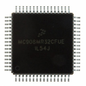
Break Motorola MC68HC908MR32 MCU
Break Motorola MC68HC908MR32 MCU is to compromise it is tamper-resistance mechanism physically and then get access to the memory zone directly, so get the mature knowledge about the definition of each PIN on the MCU is critical:
VDDA is the power supply pin for the clock generator module (CGM).
The VSSA analog ground pin is used only for the ground connections for the clock generator module (CGM) section of the circuit and should be decoupled as per the VSS digital ground pin.
The AVSS analog ground pin is used only for the ground connections for the analog to digital convertor (ADC) and should be decoupled as per the VSS digital ground pin when Recover MCU.
VREFH is the power supply for setting the reference voltage VREFH. Connect this pin to a voltage such that 1.5V < VREFH £ VDDAREF to faciliate the process of NXP Microcontroller P89LPC931 Firmware Unlocking.
The VDDAREF analog supply pin is used only for the supply connections for the analog-to-digital convertor (ADC).
CGMXFC is an external filter capacitor connection for the CGM.
PTA7–PTA0 are general-purpose bidirectional I/O port pins.
PTB7–PTB0 are special function, bidirectional port pins. PTB7–PTB0 are shared with the analog to digital convertor (ADC) input pins ATD7–ATD0.
PTC5–PTC0 are general-purpose bidirectional I/O port pins. PTC2 is a special function port pin that is shared with the system clock output pin, MCLK.
PTD7–PTD0 are general-purpose bidirectional I/O port pins. PTD6 and PTD4 are special function port pins that are shared with the timer interface modules (TIMA and TIMB).
PTE7–PTE0 are special function, bidirectional port pins. PTE7–PTE4 are shared with the serial peripheral interface mode (SPI), PTE3–PTE2 are shared with timer A (TIMA), and PTE1–PTE0 are shared with the serial communications interface (SCI).


