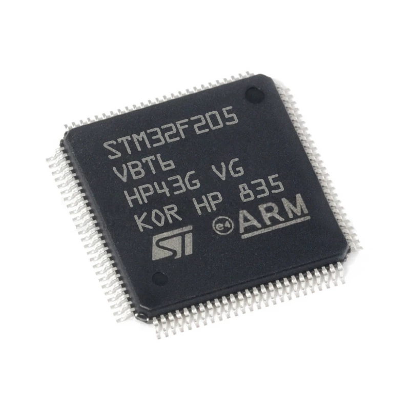
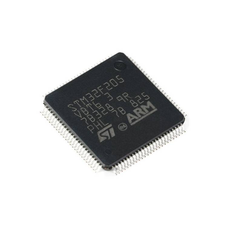
ARM Microprocessor STM32F205VB Firmware Cloning
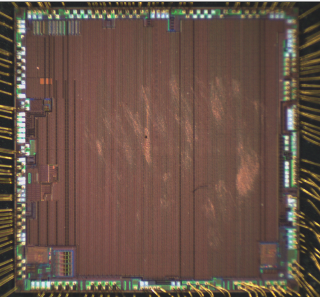
ARM Microprocessor STM32F205VB Firmware Cloning needs to attack stm32f205vb mcu chip fuse bit protection system and then extract source code from stm32f205vb controller flash memory;

At startup, boot pins are used to select one out of three boot options:
- Boot from user Flash memory
- Boot from system memory
- Boot from embedded SRAM
The boot loader is located in system memory. It is used to reprogram the Flash memory by using USART1 (PA9/PA10), USART3 (PC10/PC11 or PB10/PB11), CAN2 (PB5/PB13), USB
OTG FS in Device mode (PA11/PA12) through DFU (device firmware upgrade).
VDD = 1.8 to 3.6 V: external power supply for I/Os and the internal regulator (when enabled), provided externally through VDD pins. On devices in WLCSP64+2 package, if IRROFF is set to VDD, the supply voltage can drop to 1.7 V when the device operates
in the 0 to 70 °C temperature range using an external power supply supervisor.

VSSA, VDDA = 1.8 to 3.6 V: external analog power supplies for ADC, DAC, Reset blocks, RCs and PLL. VDDA and VSSA must be connected to VDD and VSS, respectively.
VBAT = 1.65 to 3.6 V: power supply for RTC, external clock, 32 kHz oscillator and backup registers (through power switch) when VDD is not present.
The devices have an integrated power-on reset (POR) / power-down reset (PDR) circuitry coupled with a Brownout reset (BOR) circuitry.

At power-on, POR/PDR is always active and ensures proper operation starting from 1.8 V. After the 1.8 V POR threshold level is reached to unlock stm32f205rc secured microprocessor flash program, the option byte loading process starts, either to confirm or modify default BOR threshold levels, or to disable BOR permanently. Three BOR thresholds are available through option bytes.

