-
Product Categories
Live Support Chat


Microcontroller Cracking Advancing History
It was demonstrated many times in the past how various semiconductor devices could be attacked. In the old days it was mainly non-invasive Microcontroller cracking. However, over time chip manufacturers learned the lesson and significantly improved the hardware security of their chips. This required more sophisticated methods to be used.
Modern semiconductor devices store sensitive and secret information in embedded memory. This could be passwords, encryption keys, user information or intellectual property. Therefore, devices are expected to protect both confidentiality and integrity of that information against MCU Recovery and modification.
If we look at the history of attack and defence technologies one thing could be spotted – the defence is several years behind. This becomes more evident with modern advanced deep-submicron fabrication processes. From the early 90s a common memory protection technique for smartcards was in using “invisible” ROM for code and algorithms storage.
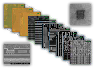
Microcontroller Cracking Advancing History
This was achieved by encoding the information with different doping level in the channels of storage transistors. As this impurities do not affect the optical properties of material, data and code extraction under optical microscopes was unsuccessful. It served well until the point when new methods were developed in Failure Analysis.
This allowed relatively inexpensive attacks to be carried out for IC code extraction. When in late 90s power analysis attacks were introduced, the semiconductor community had to take it very seriously by implementing appropriate countermeasures and performing rigorous testing on secure microcontrollers as part of their security evaluation procedure.
The discovery of the optical fault injection attacks in the early 2000s and their powerful implementation in the form of the laser fault injection forced many chip manufacturers to develop countermeasures, especially for security sensitive applications such as smartcards.