-
Product Categories
Live Support Chat


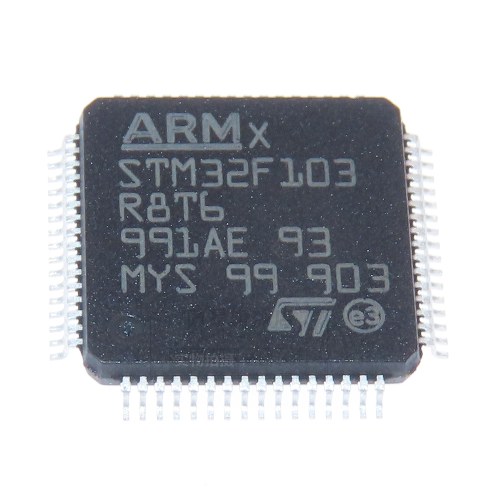
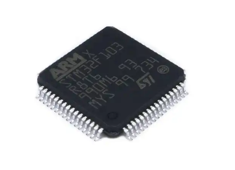
ARM Base MCU STM32F103R8 Memory Unlocking
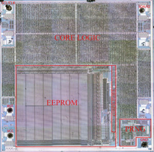
ARM-based MCU STM32F103R8 memory unlocking involves decoding and attacking the protective measures that secure its firmware stored in flash memory and EEPROM memory. This microcontroller unit (MCU) is designed with encryption and security features to prevent unauthorized access to its binary, heximal data, and embedded program. The process of unlocking the memory typically requires advanced reverse engineering techniques to bypass these protective layers and retrieve the locked firmware.
The STM32F103R8 is a widely used ARM-based microprocessor, commonly found in various embedded systems. To begin the unlocking process, engineers must first analyze the architecture of the MCU to understand the encryption methods applied to the stored data. Once the protective barriers are identified, tools and techniques are used to attack or crack the encryption, allowing access to the firmware and software embedded in the flash memory.
Decoding the binary or heximal data from the STM32F103R8 can enable the recovery of valuable information, including the source code and software necessary for system restoration or replication. This is particularly important in scenarios where the MCU is part of an obsolete or hard-to-replace system. Unlocking the memory also makes it possible to restore or clone the program, ensuring continuity of operations in critical applications.
In some cases, decrypting the firmware can also provide opportunities for further development or modification of the software, adapting it to new needs or fixing existing vulnerabilities. However, unlocking the STM32F103R8’s secured memory must be done within ethical and legal frameworks, as unauthorized access to encrypted microcomputers may violate intellectual property rights.
In conclusion, ARM-based MCU STM32F103R8 memory unlocking involves complex processes of cracking, decoding, and reverse engineering to gain access to its encrypted firmware. By bypassing security features, engineers can restore, clone, or recover critical data stored in the flash and EEPROM memory, ensuring the continued functionality of systems that rely on this protected MCU.
ARM Base MCU STM32F103R8 Memory Unlocking can disable the tamper resistance system and readout the firmware from The STM32F103R8 medium-density performance line family incorporates the high-performance ARM Cortex™-M3 32-bit RISC core operating at a 72 MHz frequency, high-speed embedded memories (Flash memory up to 128 Kbytes and SRAM up to 20 Kbytes), and an extensive range of enhanced I/Os and peripherals connected to two APB buses when carry out Microcontroller Reverse Engineering.

All devices offer two 12-bit ADCs, three general purpose 16-bit timers plus one PWM timer when Attack Microcontroller MCU Microchip PIC16F84A, as well as standard and advanced communication interfaces: up to two I2Cs and SPIs, three USARTs, an USB and a CAN.
The devices operate from a 2.0 to 3.6 V power supply. They are available in both the –40 to +85 °C temperature range and the –40 to +105 °C extended temperature range. A comprehensive set of power-saving mode allows the design of low-power applications after Crack Microprocessor IC Freescale MC9S12XDG128.
The STM32F103R8 medium-density performance line family includes devices in six different package types: from 36 pins to 100 pins. Depending on the device chosen, different sets of peripherals are included, the description below gives an overview of the complete range of peripherals proposed in this family for the purpose of Recovery Microcontroller IC NXP LPC2119FBD64.
These features make the STM32F103R8 medium-density performance line microcontroller family suitable for a wide range of applications such as motor drives, application control, medical and handheld equipment, PC and gaming peripherals, GPS platforms, industrial applications, PLCs, inverters, printers, scanners, alarm systems, video intercoms, and HVACs to facilitate the process of Unlock ARM MCU STM32F100C6 Memory.