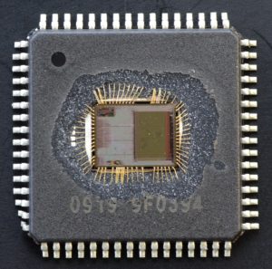
Remove MC68HC11K1 MCU Protection
This circuit is used to select either the crystal clock, CGMXCLK, or the VCO clock, CGMVCLK, as the source of the base clock, CGMOUT. The two input clocks which can be used to Remove MC68HC11K1 MCU Protection go through a transition control circuit that waits up to three CGMXCLK cycles and three CGMVCLK cycles to change from one clock source to the other.
During this time, CGMOUT is held in stasis. The output of the transition control circuit is then divided by two to correct the duty cycle by Break IC. Therefore, the bus clock frequency, which is one-half of the base clock frequency, is one-fourth the frequency of the selected clock (CGMXCLK or CGMVCLK).
The BCS bit in the PLL control register (PCTL) selects which clock drives CGMOUT. The VCO clock cannot be selected as the base clock source if the PLL is not turned on. The PLL cannot be turned off if the VCO clock is selected in order to Crack Freescale MC68HC908RK2 Flash Memory.
The PLL cannot be turned on or off simultaneously with the selection or deselection of the VCO clock. The VCO clock also cannot be selected as the base clock source if the factor L is programmed to a zero. This value would set up a condition inconsistent with the operation of the PLL, so that the PLL would be disabled and the crystal clock would be forced as the source of the base clock when Copy MC68HC05H12 Eeprom Memory Program.
The programming method Programming the PLL does not account for two possible exceptions — a value of zero for N or L is meaningless when used in the equations given. To account for these exceptions:
- A zero value for N is interpreted exactly the same as a value of one.
- A zero value for L disables the PLL and prevents its selection as the source for the base clock.


