Decode STM Chip ST7FMC1K4B6 Software
Using power supply glitch to Decode STM Chip ST7FMC1K4B6 Software has becoming more popular in the field, in the system ST7FMC1K4B6 has applied the 3.3 v internal low voltage, so in order to carry out the power supply glitch on it, we need to know the operational mechanism of internal low voltage detector,
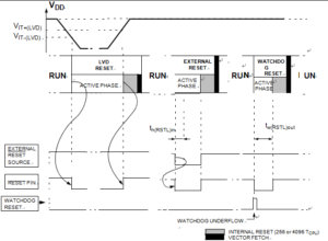
Two different RESET sequences caused by the internal LVD circuitry can be distinguished:
Power-On RESET
Voltage Drop RESET
The device RESET pin acts as an output that is pulled low when VDD<VIT+ (rising edge) or VDD<VIT- (falling edge) as shown in below Figure. The LVD filters spikes on VDD larger than tg(VDD) to avoid parasitic resets after Decode STM Chip ST7FMC1K4B6 Software.
The RESET sequence generated by a internal Watchdog counter overflow is shown in below Figure. Starting from the Watchdog counter underflow, the device RESET pin acts as an output that is pulled low during at least tw(RSTL)out.
The System Integrity Management block contains the Low Voltage Detector (LVD), Auxiliary Voltage Detector (AVD) and Clock Security System (CSS) functions. It is managed by the SICSR register when Crack STMicroelectronics MCU ST7FMC2N7BC Flash Memory. Note: A reset can also be triggered following the detection of an illegal opcode or prebyte code.
The Low Voltage Detector function (LVD) gener- ates a static reset when the VDD supply voltage is below a VIT- reference value. This means that it secures the power-up as well as the power-down keeping the ST7 in reset. The VIT- reference value for a voltage drop is lower than the VIT+ reference value for power-on in order to avoid a parasitic reset when the MCU starts running and sinks current on the supply (hysteresis) to break IC.
The LVD Reset circuitry generates a reset when VDD is below:
VIT+ when VDD is rising
VIT- when VDD is falling
The LVD function is illustrated in Figure 17.
Provided the minimum VDD value (guaranteed for the oscillator frequency) is above VIT-, the MCU can only be in two modes:
under full software control in static safe reset
In these conditions, secure operation is always ensured for the application without the need for external reset hardware. During a Low Voltage Detector Reset, the RESET pin is held low, thus permitting the MCU to reset other devices.


