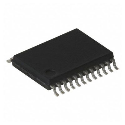
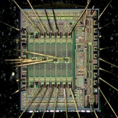
Renesas MCU R5F21192SP Flash Memory Content Cloning
Renesas MCU R5F21192SP Flash Memory Content Cloning is applying the same technique of attacking nxp LPC2119FBD64 memory, extract Microcontroller code from protective flash and eeprom memory;

This section provides information on the on-chip I/O register addresses and bit configuration. The information is given as shown below. Notes on writing to I/O registers are also given below.

I/O register addresses (address order)
Registers are listed from the lower allocation addresses.
Registers are classified according to module symbols.
Numbers of cycles for access indicate numbers of cycles of the given base clock.
Among the internal I/O register area, addresses not listed in the list of registers are reserved. Reserved addresses must not be accessed. Do not access these addresses; otherwise, the operation when accessing these bits and subsequent operations cannot be guaranteed.
Notes on writing to I/O registers

While writing to an I/O register, the CPU starts executing subsequent instructions before the I/O register write access is completed. This may cause the subsequent instructions to be executed before the write value is reflected in the operation of unlocking renesas mcu r5f211134 flash program.
The examples below show how subsequent instructions must be executed after a write access to an I/O register is completed.


