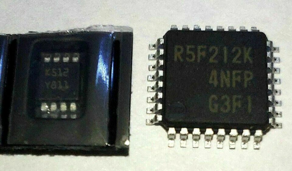
Unlock Renesas R5F21226DFP Microprocessor Flash Memory
Unlock Renesas R5F21226DFP Microprocessor Flash Memory is a process to break Renesas IC protective system and then readout the embedded firmware from microcontroller flash memory;

See Table 4.1 for details on the number of clock cycles necessary for accessing I/O registers. The number of access cycles to I/O registers is obtained by following equation.*1
Number of access cycles to I/O registers = Number of bus cycles for internal main bus 1 +
Number of divided clock synchronization cycles + Number of bus cycles for internal peripheral buses 1 to 6

The number of bus cycles of internal peripheral buses 1 to 6 differs according to the register to be accessed and the extracted firmware can be used to clone the R5F21276 microcontroller.
When peripheral functions connected to internal peripheral buses 2 to 6 or registers for the external bus control unit (except for bus error related registers) are accessed, the number of divided clock synchronization cycles is added.

The number of divided clock synchronization cycles differs depending on the frequency ratio between ICLK and PCLK (or FCLK) or bus access timing.
In the peripheral function unit, when the frequency ratio of ICLK is equal to or greater than that of PCLK (or FCLK), the sum of the number of bus cycles for internal main bus 1
And the number of the divided clock synchronization cycles will be one cycle of PCLK (or FCLK) at a maximum. Therefore, one PCLK (or FCLK) has been added to the number of access cycles shown in Table 4.1.
When the frequency ratio of ICLK is lower than that of PCLK (or FCLK), the subsequent bus access is started from the ICLK cycle following the completion of the access to the peripheral functions. Therefore, the access cycles are described on an ICLK basis.

