Unlock Microcontroller AT89C51RE2 Eeprom
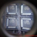
Unlock Microcontroller AT89C51RE2 Eeprom and copy the binary file from mcu at89c51re2 flash memory, the protected mcu at89c51re2 will be read after disable the protection;
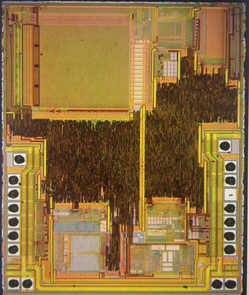
AT89C51RE2 is a high performance CMOS Flash version of the 80C51 CMOS single chip 8-bit microcontroller. It contains a 128 Kbytes Flash memory block for program.
The 128 Kbytes Flash memory can be programmed either in parallel mode or in serial mode with the ISP capability or with software. The programming voltage is internally generated from the standard VCC pin if Unlock pic18f2620 Microcontroller.
The AT89C51RE2 retains all features of the Atmel 80C52 with 256 bytes of internal RAM, a 10-source 4-level interrupt controller and three timer/counters.
In addition, the AT89C51RE2 has a Programmable Counter Array, an XRAM of 8192 bytes, a Hardware Watchdog Timer, SPI and Keyboard, two serial channels that facilitates multiprocessor communication (EUART), a speed improvement mechanism (X2 mode) and an extended stack mode that allows the stack to be extended in the lower 256 bytes of XRAM before reading pic18f4620 Microcontroller program.
The fully static design of the AT89C51RE2 allows to reduce system power consumption by bringing the clock frequency down to any value, even DC, without loss of data.
The AT89C51RE2 has 2 software-selectable modes of reduced activity and 8-bit clock prescaler for further reduction in power consumption. In the Idle mode the CPU is frozen while the peripherals and the interrupt system are still operating. In the power-down mode the RAM is saved and all other functions are inoperative.
The added features of the AT89C51RE2 make it more powerful for applications that need pulse width modulation, high speed I/O and counting capabilities such as alarms, motor control, corded phones, smart card readers if reading pic18f4585 Microcontroller heximal.
The AT89C51RE2 core needs only 6 clock periods per machine cycle. This feature called ‘X2’ provides the following advantages before Unlock Microcontroller:
Divide frequency crystals by 2 (cheaper crystals) while keeping same CPU power.
Save power consumption while keeping same CPU power (oscillator power saving).
Save power consumption by dividing dynamically the operating frequency by 2 in operating and idle modes.
Increase CPU power by 2 while keeping same crystal frequency after Unlock Microcontroller.
In order to keep the original C51 compatibility, a divider by 2 is inserted between the XTAL1 signal and the main clock input of the core (phase generator). This divider may be disabled by software when Unlock Microcontroller.
Description
The clock for the whole circuit and peripherals is first divided by two before being used by the CPU core and the peripherals.
This allows any cyclic ratio to be accepted on XTAL1 input. In X2 mode, as this divider is bypassed, the signals on XTAL1 must have a cyclic ratio between 40 to 60%.
Figure 2 shows the clock generation block diagram. X2 bit is validated on the rising edge of the XTAL1÷2 to avoid glitches when switching from X2 to STD mode. Figure 3 shows the switching mode waveforms.
Tags: unlock microcontroller heximal archive,unlock microcontroller heximal code,unlock microcontroller heximal content,unlock microcontroller heximal data,unlock microcontroller heximal eeprom,unlock microcontroller heximal file,unlock microcontroller heximal firmware,unlock microcontroller heximal information,unlock microcontroller heximal memory,unlock microcontroller heximal program


