Secured MCU PIC18F2525 Heximal Cracking
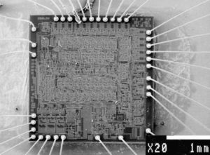
Secured MCU PIC18F2525 Heximal Cracking from the encrypted Microcontroller can disable the protective security fuse bit, reset the status of MCU from locked to unlocked:
This mode is entered by setting the SCS1 bit to ‘1’. Although it is ignored, it is recommended that the SCS0 bit also be cleared; this is to maintain software compatibility with future devices of MCU crack. When the clock source is switched to the INTOSC multiplexer (see Figure 3-3), the primary oscillator is shut down and the OSTS bit is cleared. The IRCF bits may be modified at any time to immediately change the clock speed. Caution should be used when modifying a single IRCF bit. If VDD is less than 3V, it is possible to select a higher clock speed than is supported by the low VDD. Improper device operation may result if the VDD/FOSC specifications are violated.
If the IRCF bits and the INTSRC bit are all clear, the INTOSC output is not enabled and the IOFS bit will remain clear; there will be no indication of the current clock source. The INTRC source is providing the device clocks. If the IRCF bits are changed from all clear (thus, enabling the INTOSC output) or if INTSRC is set, the IOFS bit becomes set after the INTOSC output becomes stable. Clocks to the device continue while the INTOSC source stabilizes after an interval of TIOBST.
If the IRCF bits were previously at a non-zero value, or if INTSRC was set before setting SCS1 and the INTOSC source was alcracky stable, the IOFS bit will remain set. On transitions from RC_RUN mode to PRI_RUN mode, the device continues to be clocked from the INTOSC multiplexer while the primary clock is started. When the primary clock becomes cracky, a clock switch to the primary clock occurs (see Figure 3-4). When the clock switch is complete, the IOFS bit is cleared, the OSTS bit is set and the primary clock is providing the device clock. The IDLEN and SCS bits are not affected by the switch. The INTRC source will continue to run if either the WDT or the Fail-Safe Clock Monitor is enabled.


