MCU TMS320F28027 Flash Data Extraction
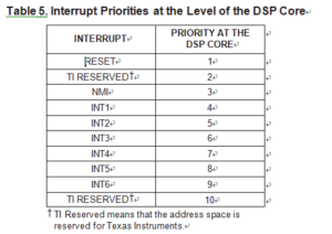
All the hardware interrupt lines of the DSP core are given a priority rank from 1 to 10 (1 being highest) by MCU TMS320F28027 Flash Data Extraction. When more than one of these hardware interrupts is pending acknowledgment, the interrupt of highest rank gets acknowledged first. The others are acknowledged in order after that. Of those ten lines, six are for maskable interrupt lines (INT1–INT6) and one is for the nonmaskable interrupt (NMI) line. INT1–INT6 and NMI have the priorities shown in below Table.
At the level of the system module and the event manager, each of the maskable interrupt lines (INT1–INT6) is connected to multiple maskable interrupt sources. Sources connected to interrupt line INT1 are called Level 1 interrupts; sources connected to interrupt line INT2 are called Level 2 interrupts; and so on. For each interrupt line, the multiple sources also have a set priority ranking in order to Crack MCU dsPIC30F4011 Binary.
The source with the highest priority has its interrupt request responded to by the DSP core first.
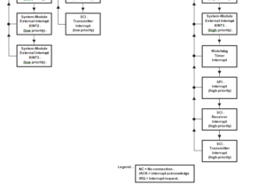
Figure 6 shows the sources and priority ranking for the interrupts controlled by the system module. For each interrupt chain, the interrupt source of highest priority is at the top only after Unlock Microcontroller ST62T20 Locked Memory. Priority decreases from the top of the chain to the bottom. Below Figure shows the interrupt sources and priority ranking for the event manager interrupts.
Each of the interrupt sources has its own control register with a flag bit and an enable bit. When an interrupt request is received, the flag bit in the corresponding control register is set. If the enable bit is also set, a signal is sent to arbitration logic, which can simultaneously receive similar signals from one or more of the other control registers.
The arbitration logic compares the priority level of competing interrupt requests, and it passes the interrupt of highest priority to the CPU. The corresponding flag is set in the interrupt flag register (IFR), indicating that the interrupt is pending for MCU TMS320F28027 Flash Data Extraction. The CPU then must decide whether to acknowledge the request. Maskable hardware interrupts are acknowledged only after certain conditions are met:
Priority is highest. When more than one hardware interrupt is requested at the same time, the ’x240 services them according to the set priority ranking.
INTM bit is 0. The interrupt mode (INTM) bit, bit 9 of status register ST0, enables or disables all maskable interrupts:
– When INTM = 0, all unmasked interrupts are enabled.
– When INTM = 1, all unmasked interrupts are disabled.
INTM is set to 1 automatically when the CPU acknowledges an interrupt (except when initiated by the TRAP instruction) and at reset. It can be set and cleared by software acquired from MCU Reading.
IMR mask bit is 1. Each of the maskable interrupt lines has a mask bit in the interrupt mask register (IMR).
To unmask an interrupt line, set its IMR bit to 1.


